


 The Marketing Minute: Cracking the Code of Technical Marketing
 Trouble in Your Tank: Implementing Direct Metallization in Advanced Substrate Packaging


Mexican Scientist in the Netherlands Seeks to Achieve Data Transmission
September 22, 2016 | Alpha GalileoEstimated reading time: 2 minutes
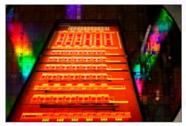
The photonic integrated circuits could replace electronic, currently used in computers or smartphones, to make them faster and compact.
In order to create effective technology that provides competitive in the market for data transmission, the mexican engineer Aura Higuera Rodriguez works in the design, manufacture and testing of dedicated optical interconnection between chips nanolasers, which ensures low power consumption and quick communication between them for sending information.
These are devices that can measure up to 300 nanometers in length, which consume low power, ie that do not generate excessive heat such as electronic devices made from silicon. "Those who we created are capable of supporting light sources and transmit data at high speed”, explained Aura Rodriguez, a doctoral student in Photonic Integration at the Technical University of Eindhoven in the Netherlands.
A single chip can contain hundreds of thousands of devices, they can be nanolasers, receivers or transmitters. These nanolasers be adapted in optical interconnects within a single chip, for example in the central processing unit of a computer or a smartphone, the purpose is to generate quick communication between chips to send information. The next generation of devices, the era of photonics.
"When we produce is like playing with a block of modeling clay, that is what we cut and molded to create and shape the laser. We ended up forming similar blocks to the lego, who put them together forms a data transmission system that uses light to carry information at high speed”, said the Telecommunications engineer from UNAM.
Is worth highlighting that these lasers are not yet marketed in the world, because, among other things, premature state in which has not reached a performance of high efficiency, difficulty in manufacturing and handling of physical properties of materials, and processing that is delicate because they are toxic materials; however, the large telecommunications companies have already announced that they will change their mode of operation to photonics, ie invest in the development of this technology because electronics no longer be viable in the future to meet the need for data transmission more speed.
Currently the investigation is under development and continuous study. "At the moment have made a chip with nanolasers, we must now characterize and check if it works technologically and then integrate it with other functions”, explained.
Despite being technology and very expensive in Mexico may apply. "You can create designs chips using specialized software, sent to Europe to manufacture and characterize a given that the necessary equipment is not expensive as used for manufacturing laboratory. It really is possible, photonics has niche opportunity and development in Mexico, you only need to start generating cooperation and seek opportunities for projects at universities and research institutes and development to consider working with technology ".
Share on:


Testimonial
"Advertising in PCB007 Magazine has been a great way to showcase our bare board testers to the right audience. The I-Connect007 team makes the process smooth and professional. We’re proud to be featured in such a trusted publication."
Klaus Koziol - atgSuggested Items
Blaize, Technology Control Company Partner to Power Saudi Arabia’s Next-Generation AI Innovation Infrastructure
09/17/2025 | BUSINESS WIREBlaize Holdings, Inc., a leader in programmable, energy-efficient edge AI computing, and Technology Control Company (TCC), a leading technology solutions provider in the Kingdom of Saudi Arabia (KSA), announced a strategic partnership to advance Saudi Arabia’s AI innovation infrastructure and accelerate its digital transformation goals.
BLT Joins Microchip Partner Program as Design Partner
09/17/2025 | BUSINESS WIREBLT, a U.S.-owned and operated engineering design services firm announced it has joined the Microchip Design Partner Program.
Curing and Verification in PCB Shadow Areas
09/17/2025 | Doug Katze, DymaxDesign engineers know a simple truth that often complicates electronics manufacturing: Light doesn’t go around corners. In densely populated PCBs, adhesives and coatings often fail to fully cure in shadowed regions created by tall ICs, connectors, relays, and tight housings.
On the Line With… Podcast: UHDI and RF Performance
09/17/2025 | I-Connect007I-Connect007 is excited to announce the release of a new episode in its latest On the Line with... podcast series, which shines a spotlight on one of the most important emerging innovations in electronics manufacturing: Ultra-High-Density Interconnect (UHDI).
Altair, Wichita State University’s NIAR Sign MoU to Accelerate Aerospace Innovation
09/16/2025 | AltairAltair, a global leader in computational intelligence, and Wichita State University’s (WSU) National Institute for Aviation Research (NIAR), one of the world’s leading aerospace research institutions, have signed a memorandum of understanding (MoU) to advance innovation across the aerospace and defense industries.