


 The Marketing Minute: Cracking the Code of Technical Marketing
 Trouble in Your Tank: Implementing Direct Metallization in Advanced Substrate Packaging


Applying Photonics to Electronic Warfare Challenges
September 23, 2016 | Georgia TechEstimated reading time: 2 minutes
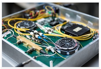
Photonics, the technology that helps drive today’s telecommunications systems, offers major advances in the area of signal transmission. Researchers at the Georgia Tech Research Institute (GTRI) are adapting optical techniques from the photonics telecom arena to enhance U.S. electronic warfare (EW) capabilities.
Optical approaches provide greatly increased frequency coverage and long distance low-loss transfer of analog signals when compared to traditional radio frequency (RF) systems, resulting in substantial performance improvements. Chip-scale integrated photonics also allows for the potential of extensive reductions in size, weight and power (SWaP) needs.
“U.S. warfighters may soon face adversary systems that use signals outside the traditional EW spectrum, which creates a need for broadband frequency responses beyond the capabilities of conventional RF and digital equipment,” said Chris Ward, a senior research engineer who leads GTRI's EW photonics development program. “Photonic advances originating in the telecom world have given us the ability to provide EW, radar and other military systems with unique and advanced performance capabilities.”
Photonics technology uses photons – particles of light – to carry wideband signals used in communications, radar and other applications over optical fiber efficiently over large distances. Photonics-based systems transmit data with far less signal loss than conventional metallic conductors, and encounter little or no electromagnetic interference while propagating through fiber.
Moreover, optical technology can be described as “frequency agnostic” – meaning a fiber-optic cable can carry signals of virtually any RF frequency, given the constraints of the electrical-to-optical and optical-to-electrical conversion process. Electric, current-carrying cables of conventional RF and digital systems can only function within narrow bandwidths on the order of gigahertz (GHz). Most optical components operate with more than 1,000 times the bandwidth, on the order of terahertz (THz).
For example, Ward explained, a user needing to process signals over 100 gigahertz (GHz) of bandwidth can easily find an optical carrier that functions at a center frequency of 193 THz, meaning that only 0.05 percent of total system bandwidth is used. By contrast, RF components using metal conductors typically consume 10 percent to 20 percent of available bandwidth per signal.
“There is an enormous benefit to operating in the optical domain.” he said. “It is typically very difficult for digital and RF electronics to cover a large spectrum instantaneously – they have to switch between multiple components in order to cover a variety of bandwidths. The engineering challenges involved in extending these traditional approaches are becoming increasingly difficult in terms of costs, schedules and SWaP. In contrast, the ability for a single optical component to perform its function over a large spectrum decreases system complexity and enables modular architectures that can be used to address future requirements.”
Today, Ward explained, sophisticated commercial off-the-shelf (COTS) photonic components, capable of cutting-edge data/signal transport, are widely available. GTRI researchers are using these devices in the development of novel EW architectures that have strong performance advantages.
Ward and his team have produced optical transceivers that can interface readily with existing digital or RF EW equipment. Employing novel photonic integrated circuits (PICs), researchers are building increased performance and flexibility into EW components. The team is currently focused on packaging PICs for integration into existing EW systems.
“There are several challenges in adapting photonics technology for highly specialized EW needs,” Ward said. “But the benefits in terms of the ability to effectively counter future threats, along with substantial cost reduction and greatly improved SWaP factors, make optical approaches highly promising for these applications.”
Share on:


Testimonial
"Our marketing partnership with I-Connect007 is already delivering. Just a day after our press release went live, we received a direct inquiry about our updated products!"
Rachael Temple - AlltematedSuggested Items
Blaize, Technology Control Company Partner to Power Saudi Arabia’s Next-Generation AI Innovation Infrastructure
09/17/2025 | BUSINESS WIREBlaize Holdings, Inc., a leader in programmable, energy-efficient edge AI computing, and Technology Control Company (TCC), a leading technology solutions provider in the Kingdom of Saudi Arabia (KSA), announced a strategic partnership to advance Saudi Arabia’s AI innovation infrastructure and accelerate its digital transformation goals.
BLT Joins Microchip Partner Program as Design Partner
09/17/2025 | BUSINESS WIREBLT, a U.S.-owned and operated engineering design services firm announced it has joined the Microchip Design Partner Program.
Curing and Verification in PCB Shadow Areas
09/17/2025 | Doug Katze, DymaxDesign engineers know a simple truth that often complicates electronics manufacturing: Light doesn’t go around corners. In densely populated PCBs, adhesives and coatings often fail to fully cure in shadowed regions created by tall ICs, connectors, relays, and tight housings.
On the Line With… Podcast: UHDI and RF Performance
09/17/2025 | I-Connect007I-Connect007 is excited to announce the release of a new episode in its latest On the Line with... podcast series, which shines a spotlight on one of the most important emerging innovations in electronics manufacturing: Ultra-High-Density Interconnect (UHDI).
Altair, Wichita State University’s NIAR Sign MoU to Accelerate Aerospace Innovation
09/16/2025 | AltairAltair, a global leader in computational intelligence, and Wichita State University’s (WSU) National Institute for Aviation Research (NIAR), one of the world’s leading aerospace research institutions, have signed a memorandum of understanding (MoU) to advance innovation across the aerospace and defense industries.