


 The Marketing Minute: Cracking the Code of Technical Marketing
 Trouble in Your Tank: Implementing Direct Metallization in Advanced Substrate Packaging


Scientists Help Create Device That Makes Monitoring Disease Biomarkers More Cost-effective
September 28, 2016 | UCLAEstimated reading time: 3 minutes
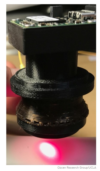
This new system weighs less than a one-tenth of a pound, making it small and light enough for a person to wear around their bicep, among other parts of their body. In the future, technology like this could be used for continuous patient monitoring at home or at point-of-care settings.
The research, which was published in the journal ACS Nano, was led by Aydogan Ozcan, UCLA’s Chancellor’s Professor of Electrical Engineering and Bioengineering and associate director of the California NanoSystems Institute and Vasiliki Demas of Verily Life Sciences (formerly Google Life Sciences).
Fluorescent biomarkers are routinely used for cancer detection and drug delivery and release among other medical therapies. Recently, biocompatible fluorescent dyes have emerged, creating new opportunities for noninvasive sensing and measuring of biomarkers through the skin.
However, detecting artificially added fluorescent objects under the skin is challenging. Collagen, melanin and other biological structures emit natural light in a process called autofluorescence. Various methods have been tried to investigate this problem using different sensing systems. Most are quite expensive and difficult to make small and cost-effective enough to be used in a wearable imaging system.
To test the mobile microscope, researchers first designed a tissue phantom — an artificially created material that mimics human skin optical properties, such as autofluorescence, absorption and scattering. The target fluorescent dye solution was injected into a micro-well with a volume of about one-hundredth of a microliter, thinner than a human hair, and subsequently implanted into the tissue phantom half a millimeter to 2 millimeters from the surface — which would be deep enough to reach blood and other tissue fluids in practice.
To measure the fluorescent dye, the wearable microscope created by Ozcan and his team used a laser to hit the skin at an angle. The fluorescent image at the surface of the skin was captured via the wearable microscope. The image was then uploaded to a computer where it was processed using a custom-designed algorithm, digitally separating the target fluorescent signal from the autofluorescence of the skin, at a very sensitive parts-per-billion level of detection.
“We can place various tiny bio-sensors inside the skin next to each other, and through our imaging system, we can tell them apart,” Ozcan said. “We can monitor all these embedded sensors inside the skin in parallel, even understand potential misalignments of the wearable imager and correct it to continuously quantify a panel of biomarkers.”
This computational imaging framework might also be used in the future to continuously monitor various chronic diseases through the skin using an implantable or injectable fluorescent dye.
Other authors of the manuscript include UCLA postdoctoral researchers Zoltan Gorocs, Yair Rivenson, Hatice Koydemir, UCLA development engineer Derek Tseng, and Tamara Troy of Verily Life Sciences.
This project was supported by Verily Life Sciences. Ozcan’s research group is supported by a Presidential Early Career Award for Scientists and Engineers, and by the Army Research Office Life Sciences Division, the National Science Foundation’s CBET Division Biophotonics Program, a National Science Foundation Emerging Frontiers in Research and Innovation award, an NSF EAGER award, an NSF INSPIRE award, the NSF Partnerships for Innovation: Building Innovation Capacity program, the Office of Naval Research, the Howard Hughes Medical Institute, the Vodaphone Americas Foundation, and King Abdullah University of Science and Technology.
Share on:


Testimonial
"Our marketing partnership with I-Connect007 is already delivering. Just a day after our press release went live, we received a direct inquiry about our updated products!"
Rachael Temple - AlltematedSuggested Items
MEMS & Imaging Sensors Summit to Spotlight Sensing Revolution for Europe’s Leadership
09/11/2025 | SEMIIndustry experts will gather November 19-20 at the SEMI MEMS & Imaging Sensors Summit 2025 to explore the latest breakthroughs in AI-driven MEMS and imaging optimization, AR/VR technologies, and advanced sensor solutions for critical defence applications.
Direct Imaging System Market Size to Hit $4.30B by 2032, Driven by Increasing Demand for High-Precision PCB Manufacturing
09/11/2025 | Globe NewswireAccording to the SNS Insider, “The Direct Imaging System Market size was valued at $2.21 Billion in 2024 and is projected to reach $4.30 Billion by 2032, growing at a CAGR of 8.68% during 2025-2032.”
I-Connect007’s Editor’s Choice: Five Must-Reads for the Week
07/04/2025 | Marcy LaRont, I-Connect007For our industry, we have seen several bullish market announcements over the past few weeks, including one this week by IDC on the massive growth in the global server market. We’re also closely watching global trade and nearshoring. One good example of successful nearshoring is Rehm Thermal Systems, which celebrates its 10th anniversary in Mexico and the official opening of its new building in Guadalajara.
Driving Innovation: Direct Imaging vs. Conventional Exposure
07/01/2025 | Simon Khesin -- Column: Driving InnovationMy first camera used Kodak film. I even experimented with developing photos in the bathroom, though I usually dropped the film off at a Kodak center and received the prints two weeks later, only to discover that some images were out of focus or poorly framed. Today, every smartphone contains a high-quality camera capable of producing stunning images instantly.
United Electronics Corporation Advances Manufacturing Capabilities with Schmoll MDI-ST Imaging Equipment
06/24/2025 | United Electronics CorporationUnited Electronics Corporation has successfully installed the advanced Schmoll MDI-ST (XL) imaging equipment at their advanced printed circuit board facility. This significant technology investment represents a continued commitment to delivering superior products and maintaining their position as an industry leader in precision PCB manufacturing.