


 The Marketing Minute: Cracking the Code of Technical Marketing
 Trouble in Your Tank: Implementing Direct Metallization in Advanced Substrate Packaging


Food Additive Key to Environmentally Friendly, Efficient, Plastic Solar Cells
September 30, 2016 | North Carolina State UniversityEstimated reading time: 1 minute
Researchers from North Carolina State University and the Chinese Academy of Sciences have created an efficient, semi-printed plastic solar cell without the use of environmentally hazardous halogen solvents. These solar cells can be manufactured at room temperature, which has implications for large-scale commercial production.
Plastic solar cells, or organic photovoltaics, are popular because they are lightweight, flexible, transparent and inexpensive to manufacture, making them useful in multiple applications. Unfortunately, the halogen-containing solvents used in their manufacture are an obstacle to large-scale commercialization. These solvents are key to making sure that the solar cell’s morphology, or structure, maximizes its energy efficiency; however, they are environmentally hazardous. Additionally, the use of these harsh chemicals requires a controlled environment, which adds to production costs.
Long Ye, a postdoctoral research scholar in physics at NC State and lead author of a paper describing the work, wanted to find out if nontoxic solvents could provide equally efficient morphology in the manufacturing process. Ye and his colleagues developed a proof of concept semi-printed plastic solar cell that utilized o-methylanisole (o-MA) as the solvent. O-MA is a commonly used flavoring agent in foods, and is nontoxic to humans.
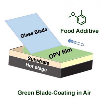
Schematic illustration and chemical structure of semi-printed plastic solar cells in air, using food additive o-MA as solvent.
Image credit: Long Ye, NC State
The researchers used soft X-ray techniques to study the morphology of their solar cell. They found that the o-MA based solar cell had similar morphology, crystalline features and device performance to those produced by halogenated solvents. The solar cell’s overall efficiency rating was around 8.4 percent. Furthermore, their cell could be produced via blade coating at ambient, or room temperature. Blade coating is a process that uses a glass blade to spread a thin layer of the photovoltaic film onto either a rigid or flexible substrate, and the process is compatible with large-scale commercial manufacturing.
“Two of the key requirements for mass producing these solar cells are that the cells can be produced in the open air environment and that the process doesn’t pose health or environmental hazards,” Ye says. “Hopefully this work can help pave the way for printing solar cells in ambient air.”
Share on:


Testimonial
"In a year when every marketing dollar mattered, I chose to keep I-Connect007 in our 2025 plan. Their commitment to high-quality, insightful content aligns with Koh Young’s values and helps readers navigate a changing industry. "
Brent Fischthal - Koh YoungSuggested Items
Alternative Manufacturing, Inc. (AMI) Announces Commitment to Excellence in Industrial, Defense, Aerospace, Renewables, and Robotics Markets
09/16/2025 | Alternative Manufacturing, Inc.Alternative Manufacturing, Inc. (AMI), a 100% employee-owned contract manufacturer, proudly reaffirms its leadership in the electronics manufacturing services (EMS) industry with a continued commitment to delivering high-quality PCBAs and box builds across the industrial, defense, aerospace, renewable energy, and robotics markets.
Sustainability and Selective Soldering
09/15/2025 | Dr. Samuel J. McMaster, Pillarhouse InternationalSustainability is more than just a buzzword for the electronics industry; it’s a key goal for all manufacturing processes. This is more than a box-ticking exercise or simply doing a small part for environmentally friendly processes. Moving toward sustainable solutions drives innovation and operational efficiency.
Trouble in Your Tank: Implementing Direct Metallization in Advanced Substrate Packaging
09/15/2025 | Michael Carano -- Column: Trouble in Your TankDirect metallization systems based on conductive graphite are gaining popularity throughout the world. The environmental and productivity gains achievable with this process are outstanding. Direct metallization reduces the costs of compliance, waste treatment, and legal issues related to chemical exposure. A graphite-based direct plate system has been devised to address these needs.
EV Group Achieves Breakthrough in Hybrid Bonding Overlay Control for Chiplet Integration
09/12/2025 | EV GroupEV Group (EVG), a leading provider of innovative process solutions and expertise serving leading-edge and future semiconductor designs and chip integration schemes, today unveiled the EVG®40 D2W—the first dedicated die-to-wafer overlay metrology platform to deliver 100 percent die overlay measurement on 300-mm wafers at high precision and speeds needed for production environments. With up to 15X higher throughput than EVG’s industry benchmark EVG®40 NT2 system designed for hybrid wafer bonding metrology, the new EVG40 D2W enables chipmakers to verify die placement accuracy and take rapid corrective action, improving process control and yield in high-volume manufacturing (HVM).
Integrating Uniplate PLBCu6 With the Digital Factory Suite
09/12/2025 | Giovanni Obino and Andreas Schatz, MKS' AtotechPrinted circuit board manufacturing is rapidly changing, driven by miniaturization, stringent reliability requirements, and growing pressure for sustainable production. Meeting these challenges requires more than incremental improvements; it demands a combination of precise equipment and real-time process intelligence. The pairing of Uniplate® PLBCu6 with the Digital Factory Suite (DFS) demonstrates how hardware and software can work together to create more responsive, resource-efficient manufacturing.