


 The Marketing Minute: Cracking the Code of Technical Marketing
 Trouble in Your Tank: Implementing Direct Metallization in Advanced Substrate Packaging


Ultra-thin Quantum LEDs Could Accelerate Development of Quantum Networks
October 10, 2016 | University of CambridgeEstimated reading time: 2 minutes
Researchers have developed all-electrical ultra-thin quantum LEDs, which have potential as on-chip photon sources in quantum information applications, including quantum networks for quantum computers.
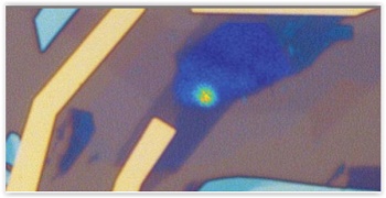
Ultra-thin quantum light emitting diodes (LEDs) – made of layered materials just a few atoms thick – have been developed by researchers at the University of Cambridge. Constructed of layers of different ultra-thin materials, the devices could be used in the development of new computing and sensing technologies. The ability to produce single photons using only electrical current is an important step towards building quantum networks on compact chips.
The devices are constructed of thin layers of different materials stacked together: graphene, boron nitride and transition metal dichalcogenides (TMDs). The TMD layer contains regions where electrons and electron vacancies, or holes, are tightly confined. When an electron fills an electron vacancy that sits at a lower energy than the electron, the energy difference is released as a photon, a particle of light. In the LED devices, a voltage pushes electrons through the device, where they fill the holes and emit single photons.
A computer built on the principles of quantum mechanics would be both far more powerful and more secure than current technologies, and would be capable of performing calculations that cannot be performed otherwise. However, in order to make such a device possible, researchers need to develop reliable methods of electrically generating single, indistinguishable photons as carriers of information across quantum networks.
The ultra-thin platform developed by the Cambridge researchers offers high levels of tunability, design freedom, and integration capabilities. Typically, single photon generation requires large-scale optical set-ups with several lasers and precise alignment of optical components. This new research brings on-chip single photon emission for quantum communication a step closer. The results are reported in the journal Nature Communications.
“Ultimately, we need fully integrated devices that we can control by electrical impulses, instead of a laser that focuses on different segments of an integrated circuit,” said Professor Mete Atatüre of Cambridge’s Cavendish Laboratory, one of the paper’s senior authors. “For quantum communication with single photons, and quantum networks between different nodes, we want to be able to just drive current and get light out. There are many emitters that are optically excitable, but only a handful are electrically driven.”
The layered nature of TMDs makes them ideal for use in ultra-thin structures on chips. They also offer an advantage over some other single-photon emitters for feasible and effective integration into nanophotonic circuits.
With this research, quantum emitters are now seen in another TMD material, namely tungsten disulphide (WS2). “We chose WS2 because we wanted to see if different materials offered different parts of the spectra for single photon emission,” said Atatüre, who is a Fellow of St John's College. “With this, we have shown that the quantum emission is not a unique feature of WS2, which suggests that many other layered materials might be able to host quantum dot-like features as well.”
“We are just scratching the surface of the many possible applications of devices prepared by combining graphene with other materials,” said senior co-author Professor Andrea Ferrari, Director of the Cambridge Graphene. “In this case, not only have we demonstrated controllable photon sources, but we have also shown that the field of quantum technologies can greatly benefit from layered materials. Many more exciting results and applications will surely follow.”
Share on:


Testimonial
"In a year when every marketing dollar mattered, I chose to keep I-Connect007 in our 2025 plan. Their commitment to high-quality, insightful content aligns with Koh Young’s values and helps readers navigate a changing industry. "
Brent Fischthal - Koh YoungSuggested Items
Curing and Verification in PCB Shadow Areas
09/17/2025 | Doug Katze, DymaxDesign engineers know a simple truth that often complicates electronics manufacturing: Light doesn’t go around corners. In densely populated PCBs, adhesives and coatings often fail to fully cure in shadowed regions created by tall ICs, connectors, relays, and tight housings.
Marcy’s Musings: Advancing the Advanced Materials Discussion
09/17/2025 | Marcy LaRont -- Column: Marcy's MusingsAs the industry’s most trusted global source of original content about the electronics supply chain, we continually ask you about your concerns, what you care about, and what you most want to learn about. Your responses are insightful and valuable. Thank you for caring enough to provide useful feedback and engage in dialogue.
September 2025 PCB007 Magazine: The Future of Advanced Materials
09/16/2025 | I-Connect007 Editorial TeamMoore’s Law is no more, and the advanced material solutions being developed to grapple with this reality are surprising, stunning, and perhaps a bit daunting. Buckle up for a dive into advanced materials and a glimpse into the next chapters of electronics manufacturing.
I-Connect007 Launches Advanced Electronics Packaging Digest
09/15/2025 | I-Connect007I-Connect007 is pleased to announce the launch of Advanced Electronics Packaging Digest (AEPD), a new monthly digital newsletter dedicated to one of the most critical and rapidly evolving areas of electronics manufacturing: advanced packaging at the interconnect level.
Panasonic Industry will Double the Production Capacity of MEGTRON Multi-layer Circuit Board Materials Over the Next Five Years
09/15/2025 | Panasonic Industry Co., Ltd.Panasonic Industry Co., Ltd., a Panasonic Group company, announced plans for a major expansion of its global production capacity for MEGTRON multi-layer circuit board materials today. The company plans to double its production over the next five years to meet growing demand in the AI server and ICT infrastructure markets.