


 The Marketing Minute: Cracking the Code of Technical Marketing
 Trouble in Your Tank: Implementing Direct Metallization in Advanced Substrate Packaging


Exploring Defects in Nanoscale Devices for Possible Quantum Computing Applications
October 19, 2016 | Tokyo Institute of TechnologyEstimated reading time: 2 minutes
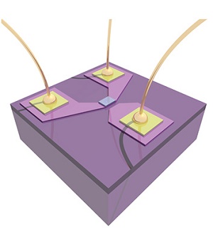
Researchers at Tokyo Institute of Technology in collaboration with the University of Cambridge have studied the interaction between microwave fields and electronic defect states inside the oxide layer of field-effect transistors at cryogenic temperatures. It has been found that the physics of such defect states are consistent with driven two-level systems possessing long coherence times, and that their induced dynamics can be coherently and independently controlled. Due to the nature of this work, it is hoped that such results will contribute to the field of correlated electronic glassy dynamics in condensed matter physics; give a better understanding of charge noise effects in mesoscopic devices; and enable new studies for developing novel technologies in the important field of semiconductor-based quantum information processing.
Defect states acting as electron traps in oxide-semiconductor interfaces usually are sources of noise and tend to reduce the performance of nanoscale devices. Such defect states can modify the electrostatic environment experienced by conducting electrons, forcing them to percolate through nanowire-like pathways at low enough temperatures. This effectively allows a detection mechanism of the occupation of such trap sites by the current measured in the conduction channel. Such effect is normally observed as random telegraph noise (RTN), which corresponds to the incoherent emission and capture of electrons in the trap states, mediated by the thermal background.
Motivated by the big changes in the conductivity caused by RTN in field-effect transistors (FET), scientists at the Quantum Nanoelectronics Research Center, Institute of Innovative Research (Tokyo Tech), the Center for Advanced Photonics and Electronics (University of Cambridge), and Cavendish Laboratory (University of Cambridge) investigated possible mechanisms in which the occupation of defects states could be both observed and dynamically mediated by means of coherent microwave fields. Working at cryogenic temperatures, it was found that the dynamics of such trap states are consistent with two-level systems (TLS), in which the energy levels are discrete and only the two lowest are accessible within the energy of the excitation signal. A TLS can represent the basis for a quantum bit implementation.
From the microwave spectroscopic signature of the response of the FET used in this work, displaying a great number of high-quality factor resonances (Q > 104), the extracted coherence times observed in this study are considerably longer, by almost three orders of magnitude, than other defect-based implementations of TLS. Performing single-pulse experiments gives the possibility to study the dynamics of the trapped electrons, which have been found not to depend on the chemistry of the dielectric used. And using a standard Ramsey protocol, coherent control was achieved. Furthermore, employing an optical master equation that captures the dynamics of the trapped electrons and a physical model based on linear response theory, it was possible to reproduce the experimental behavior observed in the experiments.
Furthermore, it was found that the defect states are relatively well protected against phonons, explaining the long decoherence times measured, and that the main source of back-action could be related to long-range Coulombic interactions with other charges. Finally, since each resonance can be addressed independently in frequency space, the wide distribution of long coherence times observed, and the quasi-uniform density of states measured, it is hoped that this work could motivate the possibility to use such systems as quantum memories or quantum bits in future quantum information processing implementations.
Share on:


Testimonial
"We’re proud to call I-Connect007 a trusted partner. Their innovative approach and industry insight made our podcast collaboration a success by connecting us with the right audience and delivering real results."
Julia McCaffrey - NCAB GroupSuggested Items
Rules of Thumb: Design007 Magazine, November 2024
11/11/2024 | I-Connect007 Editorial TeamRules of thumb are everywhere, but there may be hundreds of rules of thumb for PCB design. They’re built on design formulas, fabricators’ limitations, and tribal knowledge. And unfortunately, some longtime rules of thumb should be avoided at all costs. How do we separate the wheat from the chaff, so to speak?
Connect the Dots: Best Practices for Prototyping
09/21/2023 | Matt Stevenson -- Column: Connect the DotsPCB prototyping is a critical juncture during an electronic device’s journey from concept to reality. Regardless of a project’s complexity, the process of transforming a design into a working board is often enlightening in terms of how a design can be improved before a PCB is ready for full production.
The Drive Toward UHDI and Substrates
09/20/2023 | I-Connect007 Editorial TeamPanasonic’s Darren Hitchcock spoke with the I-Connect007 Editorial Team on the complexities of moving toward ultra HDI manufacturing. As we learn in this conversation, the number of shifting constraints relative to traditional PCB fabrication is quite large and can sometimes conflict with each other.
Asia/Pacific AI Spending Surge to Reach a Projected $78 Billion by 2027
09/19/2023 | IDCAsia/Pacific spending on Artificial Intelligence (AI) ), including software, services, and hardware for AI-centric systems will grow to $78.4 billion in 2027, according to International Data Corporation's latest Worldwide Artificial Intelligence Spending Guide.
Intel to Sell Minority Stake in IMS Nanofabrication Business to TSMC
09/13/2023 | IntelIntel Corporation announced that it has agreed to sell an approximately 10% stake in the IMS Nanofabrication business to TSMC. TSMC’s investment values IMS at approximately $4.3 billion, consistent with the valuation of the recent stake sale to Bain Capital Special Situations.