


 Trouble in Your Tank: Organic Addition Agents in Electrolytic Copper Plating
 Marcy’s Musings: Can You Hear the Voices?
 Facing the Future: Successfully Navigating the Uncertain Path Ahead


Improving Carbon Superlattices for Quantum Electronic Devices
October 21, 2016 | University of the WitwatersrandEstimated reading time: 4 minutes
Researchers at the Nanoscale Transport Physics Laboratory from the School of Physics at the University of the Witwatersrand have found a technique to improve carbon superlattices for quantum electronic device applications. Superlattices are made up of alternating layers of very thin semiconductors, just a few nanometers thick. These layers are so thin that the physics of these devices is governed by quantum mechanics, where electrons behave like waves. In a paradigm shift from conventional electronic devices, exploiting the quantum properties of superlattices holds the promise of developing new technologies.
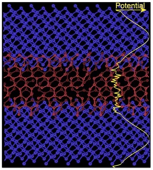
A schematic atomic diagram of a quantum well made from amorphous carbon layers. The blue atoms represent amorphous carbon with a high percentage of diamond-like carbon. The maroon atoms represent amorphous carbon which is graphite-like. The diamond-like regions have a high potential (diamond is insulating) while the graphite-like regions are more metallic. This creates a quantum well as electrons are confined within the graphite-like region due to the relatively high potential in the diamond-like regions. Superlattices are made up of a series of quantum wells. (Image: Wits University)
The group, headed by Professor Somnath Bhattacharyya has been working for the past 10 years on developing carbon-based nano-electronic devices.
"Carbon is the future in the electronics field and it soon will be challenging many other semiconductors, including silicon," says Bhattacharyya.
The physics of carbon superlattices is more complex than that of crystalline superlattices (such as gallium arsenide), since the material is amorphous and carbon atoms tend to form chains and networks. The Wits group, in association with researchers at the University of Surrey in the UK, has developed a detailed theoretical approach to understand the experimental data obtained from carbon devices. The paper has been published in Scientific Reports ("Coherent quantum transport features in carbon superlattice structures").
"This work provides an understanding of the fundamental quantum properties of carbon superlattices, which we can now use to design quantum devices for specific applications," says lead author, Wits PhD student, Ross McIntosh. "Our work provides strong impetus for future studies of the high-frequency electronic and optoelectronic properties of carbon superlattices".
Through their work, the group reported one of the first theoretical models that can explain the fundamental electronic transport properties in disordered carbon superlattices.
Bhattacharyya started looking at the use of carbon for semiconductor applications almost 10 years ago, before he joined Wits University, when he and co-authors from the University of Surrey developed and demonstrated negative differential resistance and excellent high-frequency properties of a quantum device made up of amorphous carbon layers. This work was published in Nature Materials in 2006.
McIntosh undertook the opportunity at honours level to measure the electrical properties of carbon superlattice devices. Now, as a PhD student and having worked extensively with theoretician Dr. Mikhail V. Katkov, he has extended the theoretical framework and developed a technique to calculate the transport properties of these devices.
Bhattacharyya believes this work will have immense importance in developing Carbon-based high-frequency devices.
"It will open not only fundamental studies in Carbon materials, but it will also have industrial applications in the electronic and optoelectronic device sector," he says.
A schematic atomic diagram of a quantum well made from amorphous carbon layers. The blue atoms represent amorphous carbon with a high percentage of diamond-like carbon. The maroon atoms represent amorphous carbon which is graphite-like. The diamond-like regions have a high potential (diamond is insulating) while the graphite-like regions are more metallic. This creates a quantum well as electrons are confined within the graphite-like region due to the relatively high potential in the diamond-like regions. The maroon chains through the diamond-like regions represent polymeric chains, a feature which is unique to carbon superlattices. Superlattices are made up of a series of quantum wells. The green atoms represent nitrogen impurities.
Superlattices are currently used as state of the art high frequency oscillators and amplifiers and are beginning to find use in optoelectronics as detectors and emitters in the terahertz regime. While the high frequency electrical and optoelectronic properties of conventional semiconductors are limited by the dopants used to modify their electronic properties, the properties of superlattices can be tuned over a much wider range to create devices which operate in regimes where conventional devices cannot.
Superlattice electronic devices can operate at higher frequencies and optoelectronic devices can operate at lower frequencies than their conventional counterparts. The lack of terahertz emitters and detectors has resulted in a gap in that region of the electromagnetic spectrum (known as the "terahertz gap"), which is a significant limitation, as many biological molecules are active in this regime. This also limits terahertz radio astronomy.
Amorphous Carbon devices are extremely strong, can operate at high voltages and can be developed in most laboratories in the world, without sophisticated nano-fabrication facilities. New Carbon-based devices could find application in biology, space technology, science infrastructure such as the Square Kilometre Array (SKA) telescope in South Africa, and new microwave detectors.
"What was lacking earlier was an understanding of device modelling. If we have a model, we can improve the device quality, and that is what we now have," says Bhattacharyya.
Share on:


Suggested Items
DuPont Announces Additional Directors for the Planned Independent Electronics Company
04/18/2025 | DuPontDuPont announced that Karin De Bondt and Anne Noonan will become members of the future board of directors for the independent Electronics public company that will be created following its intended spin-off from DuPont, which is targeted for November 1, 2025.
Navigating Robotics Deployment Challenges with SINBON
04/18/2025 | PRNewswireIn spite of the potential for robotics technology to expand productivity, several implementation challenges continue to stand in the way of more widespread adoption.
Can the Electronics Industry Balance Tariffs With Investment?
04/18/2025 | I-Connect007 Editorial TeamTo better understand the U.S. administration’s recent actions on global trade policies, Barry Matties and Nolan Johnson met with Richard Cappetto, IPC’s senior director of North American government relations, who highlighted both the challenges and opportunities available to U.S. companies in the recent trade activity. This could include increased domestic manufacturing and supply chain diversification.
Indium Experts to Present on Power Electronics at PCIM Europe 2025
04/17/2025 | Indium CorporationAs one of the leading materials providers to the power electronics assembly and e-Mobility industries, Indium Corporation experts will share their technical insight and knowledge on a variety of industry-related topics throughout PCIM Europe, May 6-8, in Nuremberg, Germany.
Spirit Electronics Expands U.S. Semiconductor Capacity with Acquisition of SMART Microsystems
04/17/2025 | BUSINESS WIREAs part of its strategic commitment to strengthening domestic semiconductor manufacturing, Spirit Electronics has acquired SMART Microsystems, located at Lorain County Community College (LCCC) in Ohio.