


 The Marketing Minute: Cracking the Code of Technical Marketing
 Trouble in Your Tank: Implementing Direct Metallization in Advanced Substrate Packaging


New Metamaterial Paves Way for Terahertz Technologies
October 24, 2016 | UCLAEstimated reading time: 2 minutes
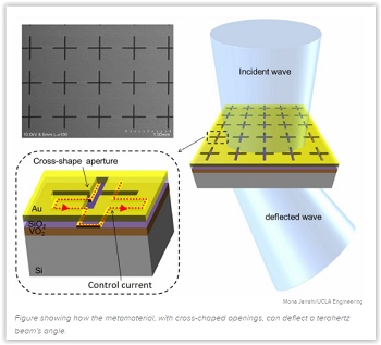
A research team led by UCLA electrical engineers has developed an artificial composite material to control of higher-frequency electromagnetic waves, such as those in the terahertz and far-infrared frequencies.
The material, specifically a metamaterial because it is has properties not found in nature, could be transformative for imaging, sensing and communication applications. It could be used for quality control in pharmaceutical production lines, scanning pills at high speeds to look for any defects; to spot cancerous tumors at early stages using tomography; or for forming adaptive high data-rate communication channels.
“Terahertz frequencies in particular offer some unique advantages, for example they can ‘see’ some details not otherwise ‘visible’ in other parts of the spectrum,” said Mona Jarrahi, an associate professor of electrical engineering at the UCLA Henry Samueli School of Engineering and Applied Science. “However their use is not widespread. Current systems require a mechanical scanning technique to steer or guide the focus area of the terahertz beam, much like a how an office copy machine uses a moving arm underneath the glass to capture an image.”
Despite extensive progress developing mechanical beam-steering techniques through miniaturization and the utilization of micro-electro mechanical systems, the potential use is still limited. Those tiny systems are complex with moving parts and for terahertz-based systems, they have not been practical. The team’s solution is simple.
“Our new metamaterial acts as a kind of moving lens that can focus on different areas of an object, but instead of being moved mechanically, its focus point is instead controlled electronically by changing an electric current that moves through it,” Jarrahi said. “The material itself never moves.”
The material is made up of metal-coated vanadium dioxide on silicon and is punctured with cross-shaped openings. It would be placed in front of the radiation beam used in an imaging or sensing application. Depending on the level of electric current, the material can deflect the beam’s focus point by as much as 44 degrees, both vertically and horizontally.
The new technology could lead to imaging, sensing and communication technologies in terahertz and far-infrared frequencies that are more reliable, compact, cost-effective and faster than the current state-of-the-art, the researchers said.
The lead author on the paper was Mohammed Reza Hashemi, a postdoctoral scholar at UCLA and member of Jarrahi’s lab. Other authors include UCLA graduate student Shang-Hua Yang; and Tongyu Wang and Nelson Sepulveda, a graduate student and an associate professor respectively, at Michigan State University’s College of Engineering.
Share on:


Testimonial
"We’re proud to call I-Connect007 a trusted partner. Their innovative approach and industry insight made our podcast collaboration a success by connecting us with the right audience and delivering real results."
Julia McCaffrey - NCAB GroupSuggested Items
BLT Joins Microchip Partner Program as Design Partner
09/17/2025 | BUSINESS WIREBLT, a U.S.-owned and operated engineering design services firm announced it has joined the Microchip Design Partner Program.
HyRel Technologies Showcases Summer Intern Success Through Hands-On Innovation
09/16/2025 | HyRel TechnologiesHyRel Technologies, a global provider of quick turn semiconductor modification solutions, proudly highlights the accomplishments of its two recent summer interns, Danny Hoang and Nisarg Jadav.
ASM Technologies Limited signs MoU with the Guidance, Government of Tamilnadu to Expand Design-Led Manufacturing capabilities for ESDM
09/15/2025 | ASM TechnologiesASM Technologies Limited, a pioneer in Design- Led Manufacturing in the semiconductor and automotive industries, announced signing of Memorandum of Understanding (MoU) with the Guidance, Government of Tamilnadu whereby it will invest Rs. 250 crores in the state to expand its ESDM related Design-Led Manufacturing and precision engineering capacity. ASM Technologies will acquire 5 acres of land from the Government of Tamilnadu to set up a state-of-the-art design facility in Tamil Nadu's growing technology manufacturing ecosystem, providing a strong strategic advantage and long-term benefits for ASM.
Intel Announces Key Leadership Appointments to Accelerate Innovation and Strengthen Execution
09/09/2025 | Intel CorporationIntel Corporation today announced a series of senior leadership appointments that support the company’s strategy to strengthen its core product business, build a trusted foundry, and foster a culture of engineering across the business.
Cadence to Acquire Hexagon’s Design & Engineering Business
09/08/2025 | Cadence Design SystemsCadence announced it has entered into a definitive agreement to acquire the Design & Engineering (D&E) business of Hexagon AB, which includes its MSC Software business—a pioneer in engineering simulation and analysis solutions.