


 The Marketing Minute: Cracking the Code of Technical Marketing
 Trouble in Your Tank: Implementing Direct Metallization in Advanced Substrate Packaging


Flexible Optical Design Method for Superconducting Nanowire Single-Photon Detectors
October 26, 2016 | NICTEstimated reading time: 2 minutes
The National Institute of Information and Communications Technology (NICT, President: Dr. Masao Sakauchi) has succeeded in the development of flexible optical design method for superconducting nanowire single-photon detectors (SSPDs or SNSPDs).
This technique enables SSPDs with a broadband high detection efficiency reject a specific wavelength, and is effective for multidisciplinary applications in fields such as the quantum cryptography, fluorescence spectroscopy, and remote sensing that require high efficiency over a precise spectral range and strong signal rejection at other wavelengths.
This achievement appeared in the Scientific Reports on October 24, 2016 ("Superconducting nanowire single-photon detectors with non-periodic dielectric multilayers"). The reported results have been partially obtained as a part of JST-SENTAN program and AMED-SENTAN program from April 2015.
Achievements
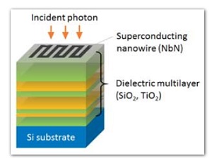
We have developed SSPDs on dielectric multilayers and their optical design method, which enable us to design a variety of wavelength dependences of optical absorptance by optimizing the dielectric multilayer.
In order to achieve the high detection efficiency in SSPDs, it is crucial to optimize the optical absorptance for a target wavelength. In the conventional SSPDs, a simple cavity structure consisting of dielectric resonant layers with a mirror layer has been used. This structure is relatively simple and can effectively achieve high absorptance at the target wavelength, and the wavelength dependencies of absorptance show a single peak structure. However, in this structure, it is difficult to realize the SSPDs with high efficiency over a carefully controlled spectral range, with rejection at other wavelengths to reduce the noises.
By adopting a new SSPD structure with dielectric multilayers, it became possible to design desired wavelength dependences of the optical absorptance. As materials of dielectric multilayer, silicon dioxide (SiO2) and titanium oxide (TiO2) were used, and the niobium nitride (NbN) superconducting nanowire was put on the dielectric multilayer. The wavelength dependences of the optical absorptance in the nanowire could be designed by optimizing the layer number and thicknesses of each layer in the dielectric multilayer. We developed the SSPDs based on the optimized design, and experimentally demonstrated that the wavelength dependences of the detection efficiency follow the calculated results well. Regarding the optical design method, in order to optimize the wavelength dependence of the absorptance effectively, we perform two-step simulation of the optical multilayer calculation and the finite element analysis.
In support of the SSPD measurements, the NICT team collaborated with Osaka University, Japan and the University of Glasgow, Scotland through the NICT internship scheme.
Future Prospects
The developed SSPD with the dielectric multilayer and the optical design method can be applied for wide wavelength region between ultraviolet and mid-infrared, and thus provides an important basis for development of application of SSPD to quantum cryptography, fluorescence spectroscopy, and remote sensing.
Share on:


Testimonial
"The I-Connect007 team is outstanding—kind, responsive, and a true marketing partner. Their design team created fresh, eye-catching ads, and their editorial support polished our content to let our brand shine. Thank you all! "
Sweeney Ng - CEE PCBSuggested Items
Accelerating Embedded Innovation: Orthogone Becomes Texas Instruments Design Partner
09/17/2025 | PRNewswireOrthogone Technologies Inc., a leader in advanced embedded systems and FPGA development, is proud to announce its official designation as a Texas Instruments (TI) Design Services Partner.
BLT Joins Microchip Partner Program as Design Partner
09/17/2025 | BUSINESS WIREBLT, a U.S.-owned and operated engineering design services firm announced it has joined the Microchip Design Partner Program.
Staying on Top of Signal Integrity Challenges
09/16/2025 | Andy Shaughnessy, Design007 MagazineOver the years, Kris Moyer has taught a variety of advanced PCB design classes, both online IPC courses and in-person classes at California State University-Sacramento, where he earned his degrees in electrical engineering. Much of his advanced curriculum focuses on signal integrity, so we asked Kris to discuss the trends he’s seeing in signal integrity today, the SI challenges facing PCB designers, and his go-to techniques for controlling or completely eliminating SI problems.
American Standard Circuits to Exhibit and Host Lunch & Learn at PCB West 2025
09/17/2025 | American Standard CircuitsAnaya Vardya, President, and CEO of American Standard Circuits/ASC Sunstone Circuits has announced that his company will once again be exhibiting at PCB West 2025 to be held at the Santa Clara Convention Center on Wednesday, October 1, 2025.
ASM Technologies Limited signs MoU with the Guidance, Government of Tamilnadu to Expand Design-Led Manufacturing capabilities for ESDM
09/15/2025 | ASM TechnologiesASM Technologies Limited, a pioneer in Design- Led Manufacturing in the semiconductor and automotive industries, announced signing of Memorandum of Understanding (MoU) with the Guidance, Government of Tamilnadu whereby it will invest Rs. 250 crores in the state to expand its ESDM related Design-Led Manufacturing and precision engineering capacity. ASM Technologies will acquire 5 acres of land from the Government of Tamilnadu to set up a state-of-the-art design facility in Tamil Nadu's growing technology manufacturing ecosystem, providing a strong strategic advantage and long-term benefits for ASM.