


 The Marketing Minute: Cracking the Code of Technical Marketing
 Trouble in Your Tank: Implementing Direct Metallization in Advanced Substrate Packaging


Improving Microscale Energy Storage Unit With Porous Materials
November 21, 2016 | King Abdullah University of Science and TechnologyEstimated reading time: 2 minutes
Microscale energy storage units for wearable and miniaturized electronic devices are improved using porous materials.
Energy storage units that can be integrated into wearable and flexible electronic systems are becoming increasingly important in today's world. A research team from KAUST has now developed a microsupercapacitor that exploits three-dimensional porous electrodes. These micropower units are expected to enable a new generation of "smart"products, such as self-powered sensors for wearables, security, structural health monitoring and "internet of things" applications.
However, for these units to be tiny yet still efficient, the highest energy density must go into the smallest area.
One approach to carrying this out is to construct microbatteries using films with a thickness of just a few micrometers or less and to replace traditional electrolytes with solid-state ones. Thin film batteries have demonstrated relatively high energy density, which is the amount of energy they can store in a given area. However, they are afflicted by limited cycle life and poor power density, meaning they are slow to charge and discharge.
Microsupercapacitors are a faster alternative, and these may prove suitable for applications requiring power pulsing and very long cycle life.
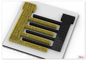
Three-dimensional porous electrodes
Three-dimensional porous electrodes could lead to smaller and efficient integrated power sources. (© Wiley)
"Also, while batteries must be charged at a constant voltage, a supercapacitor charges most efficiently by drawing the maximum current that the source can supply, irrespective of voltage," said KAUST Professor of Material Science and Engineering Husam Alshareef from the University's Functional Nanomaterials & Devices group.
This makes supercapacitors more appealing for self-powered system applications where the power source may be intermittent.
Alshareef's team has now developed integrated microsupercapacitors with vertically-scaled three-dimensional porous current collectors made from nickel foams to improve microsupercapacitor performance (Advanced Energy Materials, "Hybrid microsupercapacitors with vertically scaled 3D current collectors fabricated using a simple cut-and-transfer strategy"). The pores in the foam work to increase the surface area.
"This three-dimensional porous architecture allows excellent electrolyte permeability, good conductivity and faster ion transportation with maximum mass-loading of active material, which increase energy and power density in a given area," Alshareef said.
The microsupercapacitors were also asymmetric, using two different electrode materials for the cathode (nickel cobalt sulfide) and anode (carbon nanofiber), which nearly doubled the operating voltage. As a result, while delivering high power density (four milliwatts per square centimeter), the microsupercapacitors had an energy density of 200 microwatt-hours per square centimeter.
This is superior to state-of-the-art microsupercapacitors, which achieve between one and forty microwatt-hours per square centimeter, and is comparable to various types of thin film batteries. These high capacities were maintained even after 10,000 operating cycles.
"The high energy and power density achieve in these devices may meet the demand of on-chip storage for various types of integrated microsystems," noted KAUST Ph.D. student Qiu Jiang, the lead author of the study.
Share on:


Testimonial
"Our marketing partnership with I-Connect007 is already delivering. Just a day after our press release went live, we received a direct inquiry about our updated products!"
Rachael Temple - AlltematedSuggested Items
Rules of Thumb: Design007 Magazine, November 2024
11/11/2024 | I-Connect007 Editorial TeamRules of thumb are everywhere, but there may be hundreds of rules of thumb for PCB design. They’re built on design formulas, fabricators’ limitations, and tribal knowledge. And unfortunately, some longtime rules of thumb should be avoided at all costs. How do we separate the wheat from the chaff, so to speak?
Connect the Dots: Best Practices for Prototyping
09/21/2023 | Matt Stevenson -- Column: Connect the DotsPCB prototyping is a critical juncture during an electronic device’s journey from concept to reality. Regardless of a project’s complexity, the process of transforming a design into a working board is often enlightening in terms of how a design can be improved before a PCB is ready for full production.
The Drive Toward UHDI and Substrates
09/20/2023 | I-Connect007 Editorial TeamPanasonic’s Darren Hitchcock spoke with the I-Connect007 Editorial Team on the complexities of moving toward ultra HDI manufacturing. As we learn in this conversation, the number of shifting constraints relative to traditional PCB fabrication is quite large and can sometimes conflict with each other.
Asia/Pacific AI Spending Surge to Reach a Projected $78 Billion by 2027
09/19/2023 | IDCAsia/Pacific spending on Artificial Intelligence (AI) ), including software, services, and hardware for AI-centric systems will grow to $78.4 billion in 2027, according to International Data Corporation's latest Worldwide Artificial Intelligence Spending Guide.
Intel to Sell Minority Stake in IMS Nanofabrication Business to TSMC
09/13/2023 | IntelIntel Corporation announced that it has agreed to sell an approximately 10% stake in the IMS Nanofabrication business to TSMC. TSMC’s investment values IMS at approximately $4.3 billion, consistent with the valuation of the recent stake sale to Bain Capital Special Situations.