


 The Marketing Minute: Cracking the Code of Technical Marketing
 Trouble in Your Tank: Implementing Direct Metallization in Advanced Substrate Packaging


The Future of Electronics is Light
November 29, 2016 | University of MichiganEstimated reading time: 4 minutes
For the past four decades, the electronics industry has been driven by what is called “Moore’s Law,” which is not a law but more an axiom or observation. Effectively, it suggests that the electronic devices double in speed and capability about every two years. And indeed, every year tech companies come up with new, faster, smarter and better gadgets.
Specifically, Moore’s Law, as articulated by Intel cofounder Gordon Moore, is that “The number of transistors incorporated in a chip will approximately double every 24 months.” Transistors, tiny electrical switches, are the fundamental unit that drives all the electronic gadgets we can think of. As they get smaller, they also get faster and consume less electricity to operate.
In the technology world, one of the biggest questions of the 21st century is: How small can we make transistors? If there is a limit to how tiny they can get, we might reach a point at which we can no longer continue to make smaller, more powerful, more efficient devices. It’s an industry with more than US$200 billion in annual revenue in the U.S. alone. Might it stop growing?
Getting close to the limit
At the present, companies like Intel are mass-producing transistors 14 nanometers across – just 14 times wider than DNA molecules. They’re made of silicon, the second-most abundant material on our planet. Silicon’s atomic size is about 0.2 nanometers.
Today’s transistors are about 70 silicon atoms wide, so the possibility of making them even smaller is itself shrinking. We’re getting very close to the limit of how small we can make a transistor.
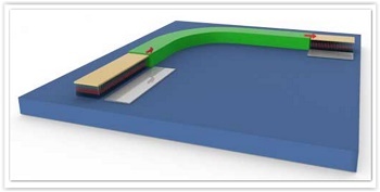
At present, transistors use electrical signals – electrons moving from one place to another – to communicate. But if we could use light, made up of photons, instead of electricity, we could make transistors even faster. My work, on finding ways to integrate light-based processing with existing chips, is part of that nascent effort.
Putting light inside a chip
A transistor has three parts; think of them as parts of a digital camera. First, information comes into the lens, analogous to a transistor’s source. Then it travels through a channel from the image sensor to the wires inside the camera. And lastly, the information is stored on the camera’s memory card, which is called a transistor’s “drain” – where the information ultimately ends up.
Right now, all of that happens by moving electrons around. To substitute light as the medium, we actually need to move photons instead. Subatomic particles like electrons and photons travel in a wave motion, vibrating up and down even as they move in one direction. The length of each wave depends on what it’s traveling through.
In silicon, the most efficient wavelength for photons is 1.3 micrometers. This is very small – a human hair is around 100 micrometers across. But electrons in silicon are even smaller – with wavelengths 50 to 1,000 times shorter than photons.
This means the equipment to handle photons needs to be bigger than the electron-handling devices we have today. So it might seem like it would force us to build larger transistors, rather than smaller ones.
However, for two reasons, we could keep chips the same size and deliver more processing power, shrink chips while providing the same power, or, potentially both. First, a photonic chip needs only a few light sources, generating photons that can then be directed around the chip with very small lenses and mirrors.
And second, light is much faster than electrons. On average photons can travel about 20 times faster than electrons in a chip. That means computers that are 20 times faster, a speed increase that would take about 15 years to achieve with current technology.
Scientists have demonstrated progress toward photonic chips in recent years. A key challenge is making sure the new light-based chips can work with all the existing electronic chips. If we’re able to figure out how to do it – or even to use light-based transistors to enhance electronic ones – we could see significant performance improvement.
When can I get a light-based laptop or smartphone?
We still have some way to go before the first consumer device reaches the market, and progress takes time. The first transistor was made in the year 1907 using vacuum tubes, which were typically between one and six inches tall (on average 100 mm). By 1947, the current type of transistor – the one that’s now just 14 nanometers across – was invented and it was 40 micrometers long (about 3,000 times longer than the current one). And in 1971 the first commercial microprocessor (the powerhouse of any electronic gadget) was 1,000 times bigger than today’s when it was released.
The vast research efforts and the consequential evolution seen in the electronics industry are only starting in the photonic industry. As a result, current electronics can perform tasks that are far more complex than the best current photonic devices. But as research proceeds, light’s capability will catch up to, and ultimately surpass, electronics’ speeds. However long it takes to get there, the future of photonics is bright.
Share on:


Testimonial
"Advertising in PCB007 Magazine has been a great way to showcase our bare board testers to the right audience. The I-Connect007 team makes the process smooth and professional. We’re proud to be featured in such a trusted publication."
Klaus Koziol - atgSuggested Items
Meet the Author Podcast: Martyn Gaudion Unpacks the Secrets of High-Speed PCB Design
07/16/2025 | I-Connect007In this special Meet the Author episode of the On the Line with… podcast, Nolan Johnson sits down with Martyn Gaudion, signal integrity expert, managing director of Polar Instruments, and three-time author in I-Connect007’s popular The Printed Circuit Designer’s Guide to... series.
Intervala Hosts Employee Car and Motorcycle Show, Benefit Nonprofits
08/27/2024 | IntervalaIntervala hosted an employee car and motorcycle show, aptly named the Vala-Cruise and it was a roaring success! Employees had the chance to show off their prized wheels, and it was incredible to see the variety and passion on display.
KIC Honored with IPC Recognition for 25 Years of Membership and Contributions to Electronics Manufacturing Industry
06/24/2024 | KICKIC, a renowned pioneer in thermal process and temperature measurement solutions for electronics manufacturing, is proud to announce that it has been recognized by IPC for 25 years of membership and significant contributions to electronics manufacturing.
Boeing Starliner Spacecraft Completes Successful Crewed Docking with International Space Station
06/07/2024 | BoeingNASA astronauts Barry "Butch" Wilmore and Sunita "Suni" Williams successfully docked Boeing's Starliner spacecraft to the International Space Station (ISS), about 26 hours after launching from Cape Canaveral Space Force Station.
KIC’s Miles Moreau to Present Profiling Basics and Best Practices at SMTA Wisconsin Chapter PCBA Profile Workshop
01/25/2024 | KICKIC, a renowned pioneer in thermal process and temperature measurement solutions for electronics manufacturing, announces that Miles Moreau, General Manager, will be a featured speaker at the SMTA Wisconsin Chapter In-Person PCBA Profile Workshop.