


 Dan’s Biz Bookshelf: ‘The Soul of a New Machine’
 The Chemical Connection: Back to Basic Cupric Chloride Etching
 The Marketing Minute: The Tyranny of the Dashboard


Graphene, the ultra-thin material just a single carbon atom in thickness, holds the promise of such impressive applications as wear-resistant, friction-free coatings. But first manufacturers have to be able to produce large sheets of graphene under precisely controlled conditions. Dirk van Baarle studied how graphene grows at atomic scale and what determines the friction with other materials. PhD defence 29 November.
Predictable quality
An almost perfectly friction-free, wear-resistant coating in machinery could generate enormous savings in fuel and maintenance. In the world of nano-technology such coatings will probably even have applications that we are currently not able to predict. In his PhD research Dirk van Baarle studied a candidate for such coatings: graphene. Van Baarle: 'It's quite a challenge to produce graphene of a predictable quality.'
Graphene is only super strong if the wire mesh of carbon atoms that make up the material are perfectly regular in form. But with the present production methods, a sheet of graphene is in practice almost always made up of a patchwork of small pieces that have been grafted onto one another. Van Baarle was able to observe almost per carbon atom live how islands of graphene grow towards one another and how this process is influenced by temperature and substrate. This is the first step towards a production method for making larger, flawless sheets of graphene.
Chicken wire pattern
Graphene occurs spontaneously when a very clean surface of iridium comes into contact with ethylene (C2H4, a hydrocarbon) at a temperature of around 700 degrees Celsius. The gas molecules disintegrate on the hot surface, leaving behind the carbon atoms, which spontaneously form a network of linked hexagons, in a chicken wire pattern.
For his research Van Baarle used a unique piece of equipment in the Huygens-Kamerlingh Onnes Laboratory, the VT-STM (Variable Temperature Scanning Tunneling Microscope). This apparatus comprises a minuscule stylus with a point that is just a few atoms thick. It can be used to systematically scan a surface with such a high degree of precision (what you are in fact doing is measuring the flow of electricity between the stylus and the surface) that even individual atoms can be distinguished. What makes the Leiden instrument unique is that it can do this even at high and variable temperatures.
A remarkable finding is that atomic processes occur not only in the growing layer of graphene. In practice, the surface of the iridium does not match the atomic layers in the substrate perfectly. The iridium forms broad steps on the surface, where the graphene grows over it. But these steps can continue to grow underneath the graphene or can withdraw as a result of the iridium atoms in the substrate realigning themselves. This process, too, has to be closely controlled in order to allow perfect sheets of graphene to form.
Contact points
In the theoretical part of his research, Van Baarle developed a model of how friction occurs at atomic level. When two surfaces slide over one another, the actual contact points are only nanometres in size, just a very few atoms. The friction is at its maximum when the stiffness of the nano-protrusions is roughly average: not too soft, but also not too stiff.
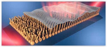
Van Baarle: 'One of my colleagues is currently coating an object with nano-needles using a lithography technique (a technique that is also used for computer chips). These needles vary in stiffness, depending on the direction in which they bend. This means that the friction of the surface is different in different directions.' This can be useful, for example, for a coating on a revolving axis, to prevent it moving laterally.
'Internally we are already using graphene coatings in our equipment to reduce friction without using lubricants,' Van Baarle explains. 'It has already resulted in a patent and a start-up, Applied Nanolayers. No wonder our professor, Joost Frenken, has already won a valorisation prize.'


