


 The Marketing Minute: Cracking the Code of Technical Marketing
 Trouble in Your Tank: Implementing Direct Metallization in Advanced Substrate Packaging


Simple Processing Technique Could Cut Cost of Organic PV and Wearable Electronics
December 6, 2016 | Georgia TechEstimated reading time: 4 minutes
A simple solution-based electrical doping technique could help reduce the cost of polymer solar cells and organic electronic devices, potentially expanding the applications for these technologies. By enabling production of efficient single-layer solar cells, the new process could help move organic photovoltaics into a new generation of wearable devices and enable small-scale distributed power generation.
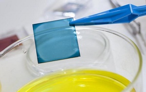
Close-up of a polymer film on a glass substrate before immersion in a polyoxometalte solution to electrically dope the film over a limited depth. Credit: Christopher Moore, Georgia Tech
Developed by researchers at the Georgia Institute of Technology and colleagues from three other institutions, the technique provides a new way of inducing p-type electrical doping in organic semiconductor films. The process involves briefly immersing the films in a solution at room temperature, and would replace a more complex technique that requires vacuum processing.
“Our hope is that this will be a game-changer for organic photovoltaics by further simplifying the process for fabricating polymer-based solar cells,” said Bernard Kippelen, director of Georgia Tech’s Center for Organic Photonics and Electronics and a professor in the School of Electrical and Computer Engineering. “We believe this technique is likely to impact many other device platforms in areas such as organic printed electronics, sensors, photodetectors and light-emitting diodes.”
Sponsored by the Office of Naval Research, the work was reported December 5 in the journal Nature Materials. The research also involved scientists from the University of California at Santa Barbara, Kyushu University in Japan, and the Eindhoven University of Technology in The Netherlands.
The technique consists of immersing thin films of organic semiconductors and their blends in polyoxometalate (PMA and PTA) solutions in nitromethane for a brief time – on the order of minutes. The diffusion of the dopant molecules into the films during immersion leads to efficient p-type electrical doping over a limited depth of 10 to 20 nanometers from the surface of the film. The p-doped regions show increased electrical conductivity and high work function, reduced solubility in the processing solvent, and improved photo-oxidation stability in air.
This new method provides a simpler alternative to air-sensitive molybdenum oxide layers used in the most efficient polymer solar cells that are generally processed using expensive vacuum equipment. When applied to polymer solar cells, the new doping method provided efficient hole collection. For the first time, single-layer polymer solar cells were demonstrated by combining this new method with spontaneous vertical phase separation of amine-containing polymers that leads to efficient electron collection at the opposing electrode. The geometry of these new devices is unique as the functions of hole and electron collection are built into the light-absorbing active layer, resulting in the simplest single-layer geometry with few interfaces.
“The realization of single-layer photovoltaics with our approach enables both electrodes in the device to be made out of low-cost conductive materials,” said Canek Fuentes-Hernandez, a senior research scientist in Kippelen’s research group. “This offers a dramatic simplification of a device geometry, and it improves the photo-oxidation stability of the donor polymer. Although lifetime and cost analysis studies are needed to assess the full impact of these innovations, they are certainly very exciting developments on the road to transform organic photovoltaics into a commercial technology.”
By simplifying the production of organic solar cells, the new processing technique could allow fabrication of solar cells in areas of Africa and Latin America that lack capital-intensive manufacturing capabilities, said Felipe Larrain, a Ph.D. student in Kippelen’s lab.
“Our goal is to further simplify the fabrication of organic solar cells to the point at which every material required to fabricate them may be included in a single kit that is offered to the public,” Larrain said. “The solar cell product may be different if you are able to provide people with a solution that would allow them to make their own solar cells. It could one day enable people to power themselves and be independent of the grid.”
Organic solar cells have been studied in many academic and industrial laboratories for several decades, and have experienced a continuous and steady improvement in their power conversion efficiency with laboratory values reaching 13 percent – compared to around 20 percent for commercial silicon-based cells. Though polymer-based cells are currently less efficient, they require less energy to produce than silicon cells and can be more easily recycled at the end of their lifetime.
“Being able to process solar cells entirely at room temperature using this simple solution-based technique could pave the way for a scalable and vacuum-free method of device fabrication, while significantly reducing the time and cost associated with it,” said Vladimir Kolesov, a Ph.D. researcher and the paper’s lead author.
Beyond solar cells, the doping technique could be more broadly used in other areas of organic electronics, noted Ph.D. researcher Wen-Fang Chou. “With its simplicity, this is truly a promising technology offering adjustable conductivity of semiconductors that could be applied to various organic electronics, and could have huge impact on the industry for mass production.”
Share on:


Testimonial
"We’re proud to call I-Connect007 a trusted partner. Their innovative approach and industry insight made our podcast collaboration a success by connecting us with the right audience and delivering real results."
Julia McCaffrey - NCAB GroupSuggested Items
Weaning the U.S. Military Off a Tablet Supply Chain That Leads to China
09/08/2025 | Jim Will, USPAETablet computers are essential to how our military fights, moves and sustains, but these devices are built on a fragile global supply chain with strong ties to China. Building domestic manufacturing to eliminate this vulnerability is feasible if we tap into the information and capabilities that already exist and create strong demand for tablets produced by trusted and assured sources.
Fresh PCB Concepts: Designing for Success at the Rigid-flex Transition Area
08/28/2025 | Team NCAB -- Column: Fresh PCB ConceptsRigid-flex PCBs come in all shapes and sizes. Manufacturers typically use fire-retardant, grade 4 (FR-4) materials in the rigid section and flexible polyimide materials in the flex region. Because of the small size, some rigid-flex PCBs, like those for hearing aid devices, are among the most challenging to manufacture. However, regardless of its size, we should not neglect the transition area between the rigid and flexible material.
Semiconductors Get Magnetic Boost with New Method from UCLA Researchers
07/31/2025 | UCLA NewsroomA new method for combining magnetic elements with semiconductors — which are vital materials for computers and other electronic devices — was unveiled by a research team led by the California NanoSystems Institute at UCLA.
Japan’s OHISAMA Project Aims to Beam Solar Power from Space This Year
07/14/2025 | I-Connect007 Editorial TeamJapan could be on the cusp of making history with its OHISAMA project in its quest to become the first country to transmit solar power from space to Earth, The Volt reported.
The Big Picture: Our Big ‘Why’ in the Age of AI
06/25/2025 | Mehul Davé -- Column: The Big PictureWith advanced technology, Tesla, Google, Microsoft, and OpenAI can quickly transform life as we know it. Several notable artificial intelligence (AI) studies, including the 2024 McKinsey Global Survey on AI, have offered insights into AI’s adoption, impact, and trajectory. The McKinsey study revealed that AI adoption continues to grow, with 50% of respondents reporting using AI in at least one business area.