


 The Marketing Minute: Cracking the Code of Technical Marketing
 Trouble in Your Tank: Implementing Direct Metallization in Advanced Substrate Packaging


UC Santa Cruz, Samsung Collaborate on Promising New Memory Technology
January 6, 2017 | University of California - Santa CruzEstimated reading time: 3 minutes
Today's computers often use as many as four different kinds of memory technology, from the hard drive to the memory chips, each with its own strengths and weaknesses. A new memory technology may be poised to disrupt this landscape, however, with a unique combination of features. It goes by the unwieldy acronym STT-MRAM, which stands for spin-transfer torque magnetic random access memory.
"All other memory technologies are good at some things and not so good at others. People are hoping that STT-MRAM can be good at everything," said electrical engineer Holger Schmidt, the Kapany Professor of Optoelectronics at UC Santa Cruz.
As one of 15 partners in the Samsung Global MRAM Innovation program, Schmidt's lab is collaborating with Samsung researchers to help develop this emerging memory technology. With his expertise in optoelectronics, Schmidt is using optical techniques based on ultra-short laser pulses to study preproduction prototype devices from Samsung. His assessments are helping the company optimize their materials and fabrication processes.
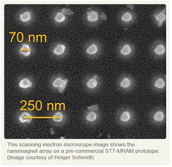
Nanomagnets
STT-MRAM stores information in the magnetic states of tiny magnetic elements or "nanomagnets" less than 100 nanometers across. Unlike other magnetic storage technologies, such as hard drives with their spinning disks and magnetic read-write heads, STT-MRAM devices have no moving parts because they use electric current to read and write data. Although current implementations still have plenty of room for improvement, the technology offers the potential for high-speed, high-density, energy-efficient memory that is nonvolatile, meaning stored information is not lost when the power is cut off.
Several key advances in physics and materials science over the past 20 years have led to the development of STT-MRAM and other so-called spintronic technologies. While electronic devices are based on the movement of electrical charges, spintronics exploits another property of electrons called spin. Spin is one of those bizarre concepts of quantum mechanics without a direct equivalent in our macroscopic world. Suffice it to say that electrons behave as if they were spinning, producing a small magnetic moment (like a tiny bar magnet with north and south poles) that can interact with other electrons and atoms in a material.
The nanomagnets in an STT-MRAM device, called spin valves or magnetic tunnel junctions, have two magnetic layers separated by a thin barrier through which electric current can flow. When the spins in the two magnetic layers are aligned, resistance is low, and if the two layers have opposite spins resistance is high, providing two readable and switchable states to represent 0 and 1 in the binary logic of computers.
Spin transfer
The ability to switch the state of a spin valve with an electric current was a critical innovation. A polarized current in which the spins of the electrons are aligned can transfer that spin state to one of the magnetic layers as it passes through, a phenomenon called spin-transfer torque (STT).
STT-MRAM chips for niche applications are just beginning to reach the market, and dozens of companies are working to optimize the technology for use in consumer electronics.
According to Schmidt, one of the challenges is to operate the chips with as little power as possible so they don't heat up too much. How much current it takes to switch a nanomagnet depends on damping, or how long it takes to settle down into a new spin state, he explained. Measuring damping parameters in an array of nanomagnets is extremely challenging, but Schmidt's lab is able to do this using short laser pulses. He and his collaborators, led by graduate student and first author Mike Jaris, reported their latest findings in a paper published in Applied Physics Letters.
"We were able to extract damping measurements from prototype devices and show the effects of the fabrication process on the material properties of the nanomagnets," Schmidt said.
The collaboration with Samsung has been exciting for his lab, he said, giving his students the opportunity to work at the cutting edge of an emerging technology. "It's a completely different type of memory, and I expect to see it used in more applications over the next few years," he said.
Share on:


Testimonial
"Our marketing partnership with I-Connect007 is already delivering. Just a day after our press release went live, we received a direct inquiry about our updated products!"
Rachael Temple - AlltematedSuggested Items
Blaize, Technology Control Company Partner to Power Saudi Arabia’s Next-Generation AI Innovation Infrastructure
09/17/2025 | BUSINESS WIREBlaize Holdings, Inc., a leader in programmable, energy-efficient edge AI computing, and Technology Control Company (TCC), a leading technology solutions provider in the Kingdom of Saudi Arabia (KSA), announced a strategic partnership to advance Saudi Arabia’s AI innovation infrastructure and accelerate its digital transformation goals.
BLT Joins Microchip Partner Program as Design Partner
09/17/2025 | BUSINESS WIREBLT, a U.S.-owned and operated engineering design services firm announced it has joined the Microchip Design Partner Program.
Curing and Verification in PCB Shadow Areas
09/17/2025 | Doug Katze, DymaxDesign engineers know a simple truth that often complicates electronics manufacturing: Light doesn’t go around corners. In densely populated PCBs, adhesives and coatings often fail to fully cure in shadowed regions created by tall ICs, connectors, relays, and tight housings.
On the Line With… Podcast: UHDI and RF Performance
09/17/2025 | I-Connect007I-Connect007 is excited to announce the release of a new episode in its latest On the Line with... podcast series, which shines a spotlight on one of the most important emerging innovations in electronics manufacturing: Ultra-High-Density Interconnect (UHDI).
Altair, Wichita State University’s NIAR Sign MoU to Accelerate Aerospace Innovation
09/16/2025 | AltairAltair, a global leader in computational intelligence, and Wichita State University’s (WSU) National Institute for Aviation Research (NIAR), one of the world’s leading aerospace research institutions, have signed a memorandum of understanding (MoU) to advance innovation across the aerospace and defense industries.