


 The Marketing Minute: Cracking the Code of Technical Marketing
 Trouble in Your Tank: Implementing Direct Metallization in Advanced Substrate Packaging


Researchers Directly Measure How Perovskite Solar Films Efficiently Convert Light to Power
January 12, 2017 | Case Western Reserve UniversityEstimated reading time: 3 minutes
Solar cells made with films mimicking the structure of the mineral perovskite are the focus of worldwide research. But only now have researchers at Case Western Reserve University directly shown the films bear a key property allowing them to efficiently convert sunlight into electricity.
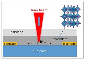
This is a schematic of scanning photocurrent imaging microscopy of halide perovskite film (side view). Using the technique, researchers found the diffusion length within a well-oriented perovskite film measured up to 20 micrometers.
Identifying that attribute could lead to more efficient solar panels.
Electrons generated when light strikes the film are unrestricted by grain boundaries -- the edges of crystalline subunits within the film -- and travel long distances without deteriorating, the researchers showed. That means electric charge carriers that become trapped and decay in other materials are instead available to be drawn off as current.
The scientists directly measured the distance traveled--called diffusion length -- for the first time by using the technique called "spatially scanned photocurrent imaging microscopy." Diffusion length within a well-oriented perovskite film measured up to 20 micrometers.
The findings, published in the journal Nano Letters ("Imaging the Long Transport Lengths of Photo-generated Carriers in Oriented Perovskite Films"), indicate that solar cells could be made thicker without harming their efficiency, said Xuan Gao, associate professor of physics and author of the paper.
"A thicker cell can absorb more light," he said, "potentially yielding a better solar cell."
Efficiency built in
Solar power researchers believe perovskite films hold great promise. In less than five years, films made with the crystalline structure have surpassed 20 percent efficiency in converting sunlight to electricity, a mark that took decades to reach with silicon-based solar cells used today.
In this research, Gao's lab performed spatially scanned photocurrent image measurements on films made in the lab of Case Western Reserve chemistry professor Clemens Burda.
Perovskite minerals found in nature are oxides of certain metals, but Burda's lab made organo-metallic films with the same crystalline structure using methyl ammonium lead tri-iodide (CH3NH3PBI3), a three-dimensional lead halide surrounded by small organic methyl ammonium molecules that hold the lattice structure together.
"The question has been, 'How are these solar cells so efficient? If we would know, we could further improve perovskite solar cells" Burda said. "People thought it could be due to unusually long electron transport, and we directly measured it."
Diffusion length is the distance an electron or its opposite, called a hole, travels from generation until it recombines or is extracted as electric current. The distance is the same as transport length when no electric field (which usually increases the distance traveled) is applied.
Measuring travel
The labs made repeated measurements by focusing a tiny laser spot on films 8 millimeters square by 300 nanometers thick. The films were made stable by coating the perovskite with a layer of the polymer parylene.
The light generates electrons and holes and the photocurrent, or stream of electrons, is recorded between the electrodes positioned about 120 microns away from each other while the film is scanned along two perpendicular directions. The scanning yields a two-dimensional spatial map of carrier diffusion and transport characteristics.
The measurements showed diffusion length averaged about 10 microns. In some cases, the length reached 20 microns, showing the functional area of the film is at least 20 microns long, the researchers said.
In some materials, grain boundaries decrease conductivity, but imaging showed that these interfaces between grains in the film exerted no influence on electron travel. Gao and Burda say this may be because grains in the film are well aligned, causing no impedance or other detrimental effects on electrons or holes.
Burda and Gao are now seeking federal funds to use the microscopy technique to determine whether different grain sizes, orientations, halide perovskite compositions, film thicknesses and more change the film's properties, to further accelerate research in the field.
Share on:


Testimonial
"We’re proud to call I-Connect007 a trusted partner. Their innovative approach and industry insight made our podcast collaboration a success by connecting us with the right audience and delivering real results."
Julia McCaffrey - NCAB GroupSuggested Items
MEMS & Imaging Sensors Summit to Spotlight Sensing Revolution for Europe’s Leadership
09/11/2025 | SEMIIndustry experts will gather November 19-20 at the SEMI MEMS & Imaging Sensors Summit 2025 to explore the latest breakthroughs in AI-driven MEMS and imaging optimization, AR/VR technologies, and advanced sensor solutions for critical defence applications.
Direct Imaging System Market Size to Hit $4.30B by 2032, Driven by Increasing Demand for High-Precision PCB Manufacturing
09/11/2025 | Globe NewswireAccording to the SNS Insider, “The Direct Imaging System Market size was valued at $2.21 Billion in 2024 and is projected to reach $4.30 Billion by 2032, growing at a CAGR of 8.68% during 2025-2032.”
I-Connect007’s Editor’s Choice: Five Must-Reads for the Week
07/04/2025 | Marcy LaRont, I-Connect007For our industry, we have seen several bullish market announcements over the past few weeks, including one this week by IDC on the massive growth in the global server market. We’re also closely watching global trade and nearshoring. One good example of successful nearshoring is Rehm Thermal Systems, which celebrates its 10th anniversary in Mexico and the official opening of its new building in Guadalajara.
Driving Innovation: Direct Imaging vs. Conventional Exposure
07/01/2025 | Simon Khesin -- Column: Driving InnovationMy first camera used Kodak film. I even experimented with developing photos in the bathroom, though I usually dropped the film off at a Kodak center and received the prints two weeks later, only to discover that some images were out of focus or poorly framed. Today, every smartphone contains a high-quality camera capable of producing stunning images instantly.
United Electronics Corporation Advances Manufacturing Capabilities with Schmoll MDI-ST Imaging Equipment
06/24/2025 | United Electronics CorporationUnited Electronics Corporation has successfully installed the advanced Schmoll MDI-ST (XL) imaging equipment at their advanced printed circuit board facility. This significant technology investment represents a continued commitment to delivering superior products and maintaining their position as an industry leader in precision PCB manufacturing.