


 The Marketing Minute: Cracking the Code of Technical Marketing
 Trouble in Your Tank: Implementing Direct Metallization in Advanced Substrate Packaging


A Bright (Nano) Light for Plasmonic Circuitry
January 13, 2017 | ICFOEstimated reading time: 2 minutes
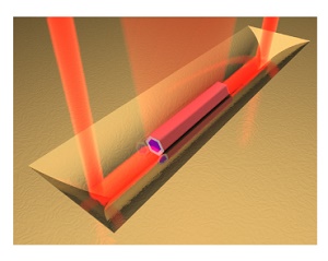
The need of ever faster and powerful data processing and communication technologies, as well as for ultrasensitive and compact sensors is playing a crucial role in the advance of novel on-chip optical devices. It is a matter of time before integrated photonic circuits will become inherent in our daily lives in a similar way that electronic circuits did with the development of the transistor. Currently, one of the main goals in nano-photonics research is being able to integrate all the key necessary building blocks on a same chip, including the light source, transmission lines, modulators and detectors. Small on-chip lasers have emerged over the last decade as an ideal solution for the light source integration, however the main challenge is to efficiently couple their emission into the small footprint components.
Now, in a recent Nanoletters publication, ICFO researcher Esteban Bermúdez-Ureña from the Plasmon Nano-optics group led by ICREA Prof. at ICFO Romain Quidant, in collaboration with the theory groups in Madrid led by Prof. Francisco J. García-Vidal and Prof. Jorge Bravo-Abad, the Laboratory for Semiconductor Materials at the EPFL in Switzerland led by Prof. Anna Fontcuberta i Morral, Dr. Cameron L.C. Smith from the TU Denmark, and Prof. Sergey I Bozhevolnyi at the Center for Nano Optics in Denmark, report on the realization of a novel ultra-compact hybrid nanolaser source operating at room temperature consisting of semiconductor nanowire (NW) lasers directly integrated with wafer-scale lithographically designed plasmonic waveguides.
To achieve this, the researchers used epitaxially grown GaAs NWs with diameters at least ten times smaller than a human hair and a few microns in length, which provided both the gain medium and the cavity geometry required for the lasing emission. The NWs were then transferred from their host substrate onto a silicon chip containing gold V-groove (VG) plasmonic waveguides, which support a special type of surface plasmons with sub-wavelength lateral electromagnetic field confinements and good propagation characteristics, namely the channel plasmon polaritons (CPPs). Later, by means of micro and nanomanipulation techniques, the researchers deterministically positioned individual NWs at the bottom of the VG channels, forming the so-called NW-VG hybrid nanolaser.
Lasing action and emission coupling to the CPP waveguide mode was observed upon pulsed illumination of the NW. Furthermore, rigorous theoretical simulations revealed that the lasing action in these devices was enabled by a hybrid photonic-plasmonic mode supported by the NW-VG geometry. The demonstrated system exhibited an unprecedented transfer efficiency of the lasing emission into the CPP waveguide mode of nearly 10%. This benchmark result was possible thanks to the good overlap between the hybrid plasmon lasing mode and the subwavelength confined CPP mode of the waveguide.
The authors envision that the unique features of the developed integrated source will provide the means to build high-sensitivity chemical or bio-sensing platforms powered by an integrated nanolaser. Future directions will also focus on the development of electrical injection as well as the integration of other on-chip components along the waveguide to build functional photonic circuitry.
Share on:


Testimonial
"In a year when every marketing dollar mattered, I chose to keep I-Connect007 in our 2025 plan. Their commitment to high-quality, insightful content aligns with Koh Young’s values and helps readers navigate a changing industry. "
Brent Fischthal - Koh YoungSuggested Items
MegaChips, Acumino Establish Demonstration Environment in Japan
09/17/2025 | BUSINESS WIREMegaChips Corporation and Acumino Inc. are pleased to announce the completion of Japan's first demonstration environment for experiencing Acumino's solutions within MegaChips' premises, signifying a strengthening of their technological collaboration.
BLT Joins Microchip Partner Program as Design Partner
09/17/2025 | BUSINESS WIREBLT, a U.S.-owned and operated engineering design services firm announced it has joined the Microchip Design Partner Program.
STMicroelectronics to Advance Next-generation Chip Manufacturing Technology with New PLP Pilot Line in Tours, France
09/17/2025 | STMicroelectronicsSTMicroelectronics, a global semiconductor leader serving customers across the spectrum of electronics applications, today announced new details regarding the development of the next generations of Panel-Level Packaging (PLP) technology through a pilot line in its Tours site, France, which is expected to be operational in Q3 2026.
Technica USA Advocates for PCBAA Membership Among Printed Circuit Assembly Customers
09/16/2025 | Technica USATechnica USA is actively encouraging its printed circuit assembly customers to join the Printed Circuit Board Association of America (PCBAA), a leading industry organization advocating for increased domestic production of printed circuit boards (PCBs) and substrates.
U.S. CHIPS Act Funding Detailed on SIA Website
09/12/2025 | Nolan Johnson, I-Connect007The U.S. CHIPS Act has moved well into the implementation stage in 2025. But where has that money gone? The Semiconductor Industry Association has been tracking these projects and provides details on its website. It was updated May. Among the five key programs being managed under CHIPS, two stand out as influencing advanced electronic packaging: the National Advanced Packaging Manufacturing Program (NAPMP), and the CHIPS Manufacturing USA Institute (MFG USA).