


 The Marketing Minute: Cracking the Code of Technical Marketing
 Trouble in Your Tank: Implementing Direct Metallization in Advanced Substrate Packaging


Nanoscale Modifications can be used to Engineer Electrical Contacts for Nanodevices
January 16, 2017 | Swansea UniversityEstimated reading time: 4 minutes
Scientists at Swansea University show nanoscale modifications to the edge region of nanocontacts to nanowires can be used to engineer the electrical transport process.
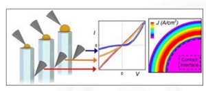
Figure 1. Schematic diagram showing the electrical measurements performed on nanowires that have different sized Au particles (left) and the resultant current-voltage behaviour (centre) is controlled by geometrical effects that determine the magnitude of tunnelling current at the contact edge, shown by finite-element simulations (right). This effect is the basis for engineering the electrical contacts. Taken from open access reference 1. Image: Alex Lord/Swansea University.
With the emergence of 1-d and 2-d nanostructures as the future of electronic materials there is a pressing need to develop new electrical contact preparation techniques that can refine the traditional processes for nanotechnological devices. The future of semiconductor devices brings significant challenges as the dimensions of the device components have been reduced from 3-d to 2-d, and now to 1-d. This research team, led by Prof. Wilks at Swansea University, is pursuing methods to engineer quantum based electrical contact technology to address the needs of the semiconductor industry as it develops devices based on nanomaterials.
Electrical contacts are essential components for any electrical device as they control the flow of electrical charge into and out of the device. When a lack of control over the final contact properties is present designing and optimising the system is impossible. Through decades of experimental and theoretical study a degree of control has been developed through band engineering when selecting contacts to large-scale planar devices such as field effect transistors. Before the advent of nanotechnology, semiconductor devices applied thin material layers to engineer interfaces and contacts, such as lasers using quantum wells, in which case the active layers could be considered 2-dimensional in nature. Now with the intense study of nanotubes, nanowires, nanorods, quantum wires, nanoribbons and many other materials the physics in some cases has been reduced to one dimension.
The current research project was expressed by Dr. Alex Lord, “New technologies based on these materials are emerging such as chemical and biological sensors, quantum computing, energy harvesting, lasers, and environmental- and photon-detectors. However, reliably engineering electrical contacts to these nanomaterials is essential to allow the development of nanoscience into a real-world technology and bring about the profound advances to the electronics industry that Scientists and Engineers know are possible.” The researcher notes that “traditional methods of engineering electrical contacts have been applied to nanomaterials but often neglect the nanoscale effects that nanoscientists have worked so hard to uncover. At the current time, a design toolbox to fabricate electrical contacts of chosen properties to nanomaterials is not close and research is lagging behind our potential application of the materials.”
The ability to define the contacts as Schottky or Ohmic with high or low resistance is complicated by the 2-d, 1-d or quasi 1-d nature of many nanomaterials and the restricted volume of material available for engineering. Traditional techniques to engineer the contact properties inevitably alter the nanomaterial properties because of the inherently large and exposed material surface.
Nanotechnology has delivered new materials and new technologies with applications of nanotechnology will continue to expand over the coming decades. Much of the usefulness stems from effects that occur at the atomic- or nano-scale. The lead researchers, Dr. Alex M. Lord and Prof. Steve Wilks at Swansea University, were motivated to “develop a deep understanding of unique effects at these length scales that occur in nanowires and to uncover synergistic relationships such as between metal nanocatalyst particles and nanowires”, said Alex Lord. There is a natural cross over between catalysts and electrical contacts because the behaviour of both can be heavily influenced by the surface properties of the material at the edge of the interface between the particle and support.
At Swansea University we have recently shown that the electrical transport of nanocatalyst contacts on nanowires can be controlled by varying the size of the metal particle in relation to the nanowire diameter, due to quantum-mechanical tunnelling at the contact edge.[1] This was confirmed in a newly-published study with UK collaborators Dr. Quentin Ramasse and Dr. Demie Kepaptsoglou at SuperSTEM, the EPSRC funded national facility for aberration-corrected STEM, UK, and also published in Nano Letters, that developed a new experimental process (eSTEM) to directly correlate atomic-resolution electron microscopy to transport measurements on single Au-nanowire interfaces.
“The new experimental procedure has a simple premise but it was challenging to optimise and allow atomic scale imaging of the interfaces. It was essential to this study and will allow many more nanomaterials to be investigated in a similar way”, said Alex Lord who developed the experiments with Quentin Ramasse. eSTEM allowed the authors to confirm the quantum effects they described earlier by adding or removing material to the tunnelling channel at the interface edge that enhances or removes the tunnelling path. This powerful effect provides a simple method for controlling the electrical transport properties of the nanocontacts that nanodevice engineers can exploit for many devices currently being developed such as nanowire biosensors.
References:
1. Lord, A. M., Ramasse, Q. M., Kepaptsoglou, D. M., Evans, J. E., Davies, P. R., Ward, M. B. & Wilks, S. P. 2016 Modifying the Interface Edge to Control the Electrical Transport Properties of Nanocontacts to Nanowires. Nano Lett. (doi:10.1021/acs.nanolett.6b03699).
2. Lord, A. M. et al. 2015 Controlling the electrical transport properties of nanocontacts to nanowires. Nano Lett. 15, 4248–4254. (doi:10.1021/nl503743t)
Share on:


Testimonial
"The I-Connect007 team is outstanding—kind, responsive, and a true marketing partner. Their design team created fresh, eye-catching ads, and their editorial support polished our content to let our brand shine. Thank you all! "
Sweeney Ng - CEE PCBSuggested Items
MEMS & Imaging Sensors Summit to Spotlight Sensing Revolution for Europe’s Leadership
09/11/2025 | SEMIIndustry experts will gather November 19-20 at the SEMI MEMS & Imaging Sensors Summit 2025 to explore the latest breakthroughs in AI-driven MEMS and imaging optimization, AR/VR technologies, and advanced sensor solutions for critical defence applications.
Direct Imaging System Market Size to Hit $4.30B by 2032, Driven by Increasing Demand for High-Precision PCB Manufacturing
09/11/2025 | Globe NewswireAccording to the SNS Insider, “The Direct Imaging System Market size was valued at $2.21 Billion in 2024 and is projected to reach $4.30 Billion by 2032, growing at a CAGR of 8.68% during 2025-2032.”
I-Connect007’s Editor’s Choice: Five Must-Reads for the Week
07/04/2025 | Marcy LaRont, I-Connect007For our industry, we have seen several bullish market announcements over the past few weeks, including one this week by IDC on the massive growth in the global server market. We’re also closely watching global trade and nearshoring. One good example of successful nearshoring is Rehm Thermal Systems, which celebrates its 10th anniversary in Mexico and the official opening of its new building in Guadalajara.
Driving Innovation: Direct Imaging vs. Conventional Exposure
07/01/2025 | Simon Khesin -- Column: Driving InnovationMy first camera used Kodak film. I even experimented with developing photos in the bathroom, though I usually dropped the film off at a Kodak center and received the prints two weeks later, only to discover that some images were out of focus or poorly framed. Today, every smartphone contains a high-quality camera capable of producing stunning images instantly.
United Electronics Corporation Advances Manufacturing Capabilities with Schmoll MDI-ST Imaging Equipment
06/24/2025 | United Electronics CorporationUnited Electronics Corporation has successfully installed the advanced Schmoll MDI-ST (XL) imaging equipment at their advanced printed circuit board facility. This significant technology investment represents a continued commitment to delivering superior products and maintaining their position as an industry leader in precision PCB manufacturing.