


 The Marketing Minute: Cracking the Code of Technical Marketing
 Trouble in Your Tank: Implementing Direct Metallization in Advanced Substrate Packaging


A Big Nano Boost for Solar Cells
January 23, 2017 | Kyoto UniversityEstimated reading time: 2 minutes
Solar cells convert light into electricity. While the sun is one source of light, the burning of natural resources like oil and natural gas can also be harnessed.
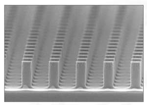
A Kyoto University and Osaka Gas silicon device could double the energy conversion rate of solar cells. Each vertical rod measures about 500 nm in height. CREDIT Kyoto University/Noda Lab
However, solar cells do not convert all light to power equally, which has inspired a joint industry-academia effort to develop a potentially game-changing solution.
"Current solar cells are not good at converting visible light to electrical power. The best efficiency is only around 20%," explains Kyoto University's Takashi Asano, who uses optical technologies to improve energy production.
Higher temperatures emit light at shorter wavelengths, which is why the flame of a gas burner will shift from red to blue as the heat increases. The higher heat offers more energy, making short wavelengths an important target in the design of solar cells.
"The problem," continues Asano, "is that heat dissipates light of all wavelengths, but a solar cell will only work in a narrow range.
"To solve this, we built a new nano-sized semiconductor that narrows the wavelength bandwidth to concentrate the energy."
Previously, Asano and colleagues of the Susumu Noda lab had taken a different approach. "Our first device worked at high wavelengths, but to narrow output for visible light required a new strategy, which is why we shifted to intrinsic silicon in this current collaboration with Osaka Gas," says Asano.
To emit visible wavelengths, a temperature of 1000C was needed, but conveniently silicon has a melting temperature of over 1400C. The scientists etched silicon plates to have a large number of identical and equidistantly-spaced rods, the height, radii, and spacing of which was optimized for the target bandwidth.
According to Asano, "the cylinders determined the emissivity," describing the wavelengths emitted by the heated device.
Using this material, the team has shown in Science Advances that their nanoscale semiconductor raises the energy conversion rate of solar cells to at least 40%.
"Our technology has two important benefits," adds lab head Noda. "First is energy efficiency: we can convert heat into electricity much more efficiently than before. Secondly is design. We can now create much smaller and more robust transducers, which will be beneficial in a wide range of applications."
About Kyoto University
Kyoto University is one of Japan and Asia's premier research institutions, founded in 1897 and responsible for producing numerous Nobel laureates and winners of other prestigious international prizes. A broad curriculum across the arts and sciences at both undergraduate and graduate levels is complemented by numerous research centers, as well as facilities and offices around Japan and the world.
Share on:


Testimonial
"Advertising in PCB007 Magazine has been a great way to showcase our bare board testers to the right audience. The I-Connect007 team makes the process smooth and professional. We’re proud to be featured in such a trusted publication."
Klaus Koziol - atgSuggested Items
Rules of Thumb: Design007 Magazine, November 2024
11/11/2024 | I-Connect007 Editorial TeamRules of thumb are everywhere, but there may be hundreds of rules of thumb for PCB design. They’re built on design formulas, fabricators’ limitations, and tribal knowledge. And unfortunately, some longtime rules of thumb should be avoided at all costs. How do we separate the wheat from the chaff, so to speak?
Connect the Dots: Best Practices for Prototyping
09/21/2023 | Matt Stevenson -- Column: Connect the DotsPCB prototyping is a critical juncture during an electronic device’s journey from concept to reality. Regardless of a project’s complexity, the process of transforming a design into a working board is often enlightening in terms of how a design can be improved before a PCB is ready for full production.
The Drive Toward UHDI and Substrates
09/20/2023 | I-Connect007 Editorial TeamPanasonic’s Darren Hitchcock spoke with the I-Connect007 Editorial Team on the complexities of moving toward ultra HDI manufacturing. As we learn in this conversation, the number of shifting constraints relative to traditional PCB fabrication is quite large and can sometimes conflict with each other.
Asia/Pacific AI Spending Surge to Reach a Projected $78 Billion by 2027
09/19/2023 | IDCAsia/Pacific spending on Artificial Intelligence (AI) ), including software, services, and hardware for AI-centric systems will grow to $78.4 billion in 2027, according to International Data Corporation's latest Worldwide Artificial Intelligence Spending Guide.
Intel to Sell Minority Stake in IMS Nanofabrication Business to TSMC
09/13/2023 | IntelIntel Corporation announced that it has agreed to sell an approximately 10% stake in the IMS Nanofabrication business to TSMC. TSMC’s investment values IMS at approximately $4.3 billion, consistent with the valuation of the recent stake sale to Bain Capital Special Situations.