


 The Marketing Minute: Cracking the Code of Technical Marketing
 Trouble in Your Tank: Implementing Direct Metallization in Advanced Substrate Packaging


NASA Advances First-Ever Silicon-Based X-ray Optic
February 8, 2017 | NASAEstimated reading time: 4 minutes
Zhang, an astrophysicist at NASA’s Goddard Space Flight Center in Greenbelt, Maryland, has shown in repeated testing that single-crystal silicon — a hard, brittle non-metallic element used in the manufacturing of computer chips — works exceptionally well as an X-ray optic.
Given the cost of building space observatories — which only increase in price as they get larger and heavier — the goal is to develop easily reproducible lightweight optics, without sacrificing quality. According to Zhang, use of silicon would give X-ray astrophysicists what they have long wanted: lightweight, super-thin mirrors that offer a significantly larger collection area and dramatically improved resolution — all at a reduced cost, Zhang said.
To date, no one has created an X-ray mirror that addresses all these performance goals. Furthermore, no one has polished and figured silicon for X-ray optics, which must be curved and nested inside a canister-like assembly to collect highly energetic X-ray photons. With this special configuration, X-rays graze the mirrors’ surfaces — like how a thrown pebble skims across the surface of a pond — rather than passing through them.
Silicon, which doesn’t warp even when cut or exposed to fluctuating temperatures, offers a viable solution, Zhang said. “We have executed our mirror-making procedures many times,” he added. “These represent the best lightweight X-ray mirrors ever. As a matter of fact, of all the astronomical X-ray mirrors that have been produced and flown, only Chandra’s are better,” he said, referring to one of NASA’s Great Observatories, an X-ray mission that carries the highest-resolution X-ray mirrors ever launched. “But we aspire to match and then exceed Chandra’s mirror quality before 2020.”
Zhang intends to achieve that goal, in part, with NASA Strategic Astrophysics Technology funding. He and his team plan to further advance the non-conventional technology in preparation for a future X-ray mission.
Old Hand at Mirror Making
Zhang is not a newcomer to the mirror-making business.
Fifteen years ago, he set out to develop a less-expensive, more efficient technique for crafting lightweight X-ray mirrors. He succeeded. Four years ago, he delivered 9,000 super-thin, curved glass mirrors for NASA’s Nuclear Spectroscopic Telescope Array, or NuSTAR, mission using a novel manufacturing technique in which he placed thin pieces of commercially available glass on a mandrel and heated the entire assembly inside an oven — a process called slumping. As the glass heated, it softened and folded over the mandrel to produce a curved mirror that the Copenhagen-based Danish Technical University then coated with layers of silicon and tungsten to maximize its X-ray reflectance.
Taking it to the Limit
Though Zhang proved the technique and produced thousands of modest-resolution mirrors ideal for NuSTAR, Zhang realized that he had taken the approach to its limit. “I spent a couple years trying to make slumped glass better. I got all the mileage I could get.”
He got rid of eight of his 10 ovens used in the slumping process and turned his attention, instead, to single-crystal silicon.
Unbeknownst to him, another Goddard technologist, Vince Bly, had already investigated the material’s use, ultimately producing a thick, yet lightweight spare mirror for the Goddard-built Thermal Infrared Sensor, one of two instruments developed for NASA’s Landsat Data Continuity Mission. Though the mission didn’t use the mirror because the optic had never flown in space, Bly said testing indicated that it offered a viable option.
When Zhang heard about Bly’s work, he and Bly started working together, benefiting from each other’s experience. “He used what we had done to solve his own problem,” Bly said.
No-Stress Silicon
The key, both said, lies with the material itself. Traditional materials for making mirrors — glass, ceramics, and metals — suffer from high internal stress, especially when cut or exposed to changing temperatures. These stresses become increasingly unpredictable as the mirror becomes thinner.
“Single crystal silicon is an excellent material for making spaceflight X-ray mirrors,” Zhang said. “It is inexpensive and abundantly available because of the semiconductor industry. Furthermore, it is a perfect material. It is immune from the internal stresses that can change the shape of X-ray mirrors made of glass.”
This is because every atom is arranged in a lattice configuration, which prevents the material from distorting even when cut or shaped. In other words, if a sheet of plywood were made of silicon, it would be perfectly flat and immune from warping, he said.
Learned from Slumping
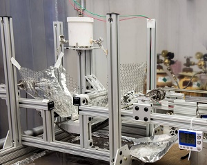
Zhang’s new process grows out of what he learned through glass slumping, he said. He takes a block of silicon and heats it to eliminate any stress that may have arisen from its handling. With a band saw, he creates the approximate shape and uses other machining tools and chemicals to further grind and refine the block’s surface. Like slicing cheese, he then cuts a thin substrate measuring just a fraction of an inch in thickness from the block and polishes the surface. The last step is coating the individual segments with iridium to improve reflectance.
With his NASA funding, Zhang and his team are perfecting techniques for aligning and bonding 6,000 mirror segments to form meta-shells that would be integrated inside a mirror assembly projected to weigh about 200 pounds and stand just a 1.6-feet tall. Ultimately, he would like to create six meta-shells and automate the alignment process.
“Making lightweight, high-resolution, relatively inexpensive X-ray mirrors has become my life’s work,” Zhang said, referring to his quest to develop a lighter, more capable X-ray mirror. “When I started developing mirrors 15 years ago, I thought I’d get it done in a couple years. Fifteen years later, I’m still at it,” Zhang said.
Share on:


Testimonial
"Advertising in PCB007 Magazine has been a great way to showcase our bare board testers to the right audience. The I-Connect007 team makes the process smooth and professional. We’re proud to be featured in such a trusted publication."
Klaus Koziol - atgSuggested Items
Rules of Thumb: Design007 Magazine, November 2024
11/11/2024 | I-Connect007 Editorial TeamRules of thumb are everywhere, but there may be hundreds of rules of thumb for PCB design. They’re built on design formulas, fabricators’ limitations, and tribal knowledge. And unfortunately, some longtime rules of thumb should be avoided at all costs. How do we separate the wheat from the chaff, so to speak?
Connect the Dots: Best Practices for Prototyping
09/21/2023 | Matt Stevenson -- Column: Connect the DotsPCB prototyping is a critical juncture during an electronic device’s journey from concept to reality. Regardless of a project’s complexity, the process of transforming a design into a working board is often enlightening in terms of how a design can be improved before a PCB is ready for full production.
The Drive Toward UHDI and Substrates
09/20/2023 | I-Connect007 Editorial TeamPanasonic’s Darren Hitchcock spoke with the I-Connect007 Editorial Team on the complexities of moving toward ultra HDI manufacturing. As we learn in this conversation, the number of shifting constraints relative to traditional PCB fabrication is quite large and can sometimes conflict with each other.
Asia/Pacific AI Spending Surge to Reach a Projected $78 Billion by 2027
09/19/2023 | IDCAsia/Pacific spending on Artificial Intelligence (AI) ), including software, services, and hardware for AI-centric systems will grow to $78.4 billion in 2027, according to International Data Corporation's latest Worldwide Artificial Intelligence Spending Guide.
Intel to Sell Minority Stake in IMS Nanofabrication Business to TSMC
09/13/2023 | IntelIntel Corporation announced that it has agreed to sell an approximately 10% stake in the IMS Nanofabrication business to TSMC. TSMC’s investment values IMS at approximately $4.3 billion, consistent with the valuation of the recent stake sale to Bain Capital Special Situations.