


 American Made Advocacy: Five Years of Educating, Advocating, and Influencing Legislation and Policy
 Defense Speak Interpreted: Understanding What the Department of Defense Is, and Isn’t
 The Right Approach: The End of an Era—DoD Proposes MIL-PRF-31032 Cancellation


The University of Bristol has been awarded a £4.3 million grant from the Engineering and Physical Sciences Research Council (EPSRC) to lead an important new project to develop Gallium Nitride (GaN)-on-Diamond microwave technology.
This next generation technology will underpin future high power radio frequency and microwave communications, space and defence systems, paving the way towards 5G and 6G mobile phone networks and much more comprehensive radar systems. Bristol will work with a consortium of four other universities (Cardiff, Glasgow, Cambridge and Birmingham) and leading industry partners during this five-year project.
Professor Martin Kuball, from the School of Physics at Bristol, is leading this project. He said: "Global demand for high power microwave electronic devices that can deliver power densities well exceeding current technology is increasing.
"In particular Gallium Nitride (GaN) based high electron mobility transistors (HEMTs) are a key enabling technology for high-efficiency military and civilian microwave systems, and increasingly for renewable energy plants."
For example information in a mobile communication systems is transmitted as ‘0’ and ‘1’s, so-called bits, and per bit this requires a certain amount of energy. In 5G, the number of bits transmitted per second will be immense, and future systems will ask for even more; current microwave devices which are used to transmit these bits in 4G networks do not have the muscle and power needed.
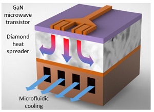
The vision of this new project is to develop transformative GaN-on-Diamond HEMTs and monolithic microwave integrated circuits (MMICs), the technology step beyond current microwave devices.
Energy flows in these can be as high as the heat flux on the surface of the sun, and the diamond with its ultra-high thermal conductivity is the only material which can handle them. These devices will allow the implementation of future communications networks and radar systems with capabilities beyond what is presently possible.
Professor Kuball added: "To enable our vision to become reality, we will develop new diamond growth approaches that maximize diamond thermal conductivity close to the active GaN device area. In present research GaN-on-Diamond devices a thin dielectric layer is required on the GaN surface to enable seeding and successful deposition of diamond onto the GaN. Unfortunately, most of the thermal barrier in these devices then exists at this GaN-dielectric-diamond interface, which has much poorer thermal conductivity than desired.
"Any reduction in this thermal resistance, either by removing the need for a dielectric seeding layer for diamond growth, or by optimizing the grain structure of the diamond near the seeding, would be of huge benefit. Novel diamond growth will be combined with innovative micro-fluidics using phase-change materials, a dramatically more powerful approach than conventional micro-fluidics, to further aid heat extraction."
The outcome will be devices with a spectacular >5x increase in RF power compared to the current state-of-the-art GaN-on-silicon carbide HEMTs, presently commercially available. Alternatively and equally valuably, a dramatic 'step-change' shrinkage in MMIC or power amplifier (PA) size is possible, delivering an increase in efficiency through the removal of combining networks as well as a reduction in power amplifier cost. This represents a disruptive change in capability that will allow the realisation of new system architectures – for example, for radio frequency seekers and medical applications, and enable the bandwidths needed to deliver 5G and beyond. Reduced requirements for cooling/increased reliability will result in major cost savings at the system level.


