


 The Marketing Minute: Cracking the Code of Technical Marketing
 Trouble in Your Tank: Implementing Direct Metallization in Advanced Substrate Packaging


Frequency Combs: On-Chip Integration on Track
February 15, 2017 | EPFLEstimated reading time: 2 minutes
EPFL scientists have found a way to miniaturize frequency combs, realizing a new step toward miniaturization of such tools. Their device can measure light oscillations with a precision of 12 digits.
A compact, precision tool for counting and tracking laser frequencies may improve atomic clocks and optical data transmission devices. However, light waves oscillate hundreds of trillions of times per second, a frequency that is impossible to measure directly. Large pulsed laser sources are typically used to produce “frequency combs” that can link the optical domain to the radio frequencies and make counting the oscillations of light possible. EPFL scientists have found a way to miniaturize frequency combs, realizing a new step toward miniaturization of such tools. Their device was capable of measuring light oscillations with a precision of 12 digits. The work is published in the journal Light: Science and Applications.
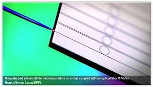
The lab of Tobias J. Kippenberg at EPFL, in a project led by Victor Brasch and Erwan Lucas, created what is called a “self-referenced optical frequency comb”. This is essentially a series of densely-spaced spectral lines whose spacing is identical and known. Because they are so well defined, optical frequency combs can be used as a “ruler” for measuring the frequency – or color – of any laser beam. By comparing an unknown color to this ruler, it is possible to calculate its frequency. However, this implies a critical step called “self-referencing”, a method that exactly determines the position of each individual tick of the frequency ruler, but demands a very long ruler – a broad spectral range, as scientists say – which is challenging to obtain.
Although optical frequency combs earned their inventors the Nobel prize in Physics in 2005, they still required bulky optical setups. Prof. Kippenberg’s lab showed in 2007 that optical frequency combs could be created using tiny devices called “optical microresonators”: microscopic ring-shaped structures made from very fine silicon nitride measuring a few millimeters to a few tens of microns in diameter. These structures can trap a continuous laser light and convert it into ultra-short pulses – solitons – thanks to the special nonlinear properties of the device. The solitons travel around the microresonator 200 billion times per second and the pulsed output from the microresonator creates the optical frequency comb.
Last year, the group solved an outstanding challenge, demonstrating that a careful control of the microresonator parameters, enabled to generate a very broad frequency spectrum directly on-chip. At this point, the frequencies generated extend over two thirds of an octave compared with the frequency of the incoming laser (an octave refers to either double or half the frequency). When combined with a laser transfer system, based on non-linear crystals, the team’s approach enabled self-referencing, while eliminating the need for bulky, external systems traditionally used for frequency broadening.
With this, the researchers could prove that their optical frequency comb can be used for the most precise measurement applications: they measured the frequency of a laser using their technique as well as a traditional frequency comb system and showed that the two results agreed over 12 digits.
The technology is amenable to integration with both photonic elements and silicon microchips. Establishing devices that provide a RF to optical link on a chip may catalyze a wide variety of applications such as integrated, atomic clocks and on-chip, and could contribute to making optical frequency metrology ubiquitous.
Share on:


Testimonial
"Advertising in PCB007 Magazine has been a great way to showcase our bare board testers to the right audience. The I-Connect007 team makes the process smooth and professional. We’re proud to be featured in such a trusted publication."
Klaus Koziol - atgSuggested Items
U.S. Uses Secret Trackers to Trace AI Chips Diverted to China, Sources Say
08/18/2025 | I-Connect007 Editorial TeamTwo sources told Reuters that U.S. authorities have secretly placed location trackers in some advanced chip shipments they see as at high risk of illegal diversion to China. They said the trackers are intended to locate AI chips that are sent to locations restricted by U.S. export laws, but authorities only examine some shipments.
Happy’s Tech Talk #38: Novel Metallization for UHDI
05/07/2025 | Happy Holden -- Column: Happy’s Tech TalkI have been involved in high-density electronics substrates since 1970 when I joined Hewlett-Packard’s RF semiconductor group after college. Figure 1 shows the difference between trace/space lithography for substrates and silicon starting in 1970. My projects involved sapphire circuits for RF devices, but the figure displays the state of PCBs and integrated CMOS circuits and their packaging, not discreet RF devices. Even then, semiconductors were 50X higher density.
New Database of Materials Accelerates Electronics Innovation
05/05/2025 | ACN NewswireIn a collaboration between Murata Manufacturing Co., Ltd., and the National Institute for Materials Science (NIMS), researchers have built a comprehensive new database of dielectric material properties curated from thousands of scientific papers.
New Database of Materials Accelerates Electronics Innovation
05/02/2025 | ACN NewswireIn a collaboration between Murata Manufacturing Co., Ltd., and the National Institute for Materials Science (NIMS), researchers have built a comprehensive new database of dielectric material properties curated from thousands of scientific papers.
Micron Announces Business Unit Reorganization to Capitalize on AI Growth Across All Market Segments
04/23/2025 | MicronMicron Technology, Inc., a leader in innovative memory and storage solutions, announced a market segment-based reorganization of its business units to capitalize on the transformative growth driven by AI, from data centers to edge devices.