


 Dan’s Biz Bookshelf: ‘Elevate: Push Beyond Your Limits'
 The Marketing Minute: The First Step to More Sales—Marketing
 It’s Only Common Sense: Customer Service Is Sales in Disguise


AT&S Advances PCB, Module and Packaging Technologies
March 1, 2017 | AT&SEstimated reading time: 2 minutes
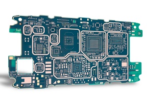
For years, AT&S has worked at the forefront of process and technology development to meet the challenges of continued miniaturization and the demand for better energy efficiency. In this context, the company is involved in various research and development programmes. One current example is the Horizon 2020 EU Research and Innovation programme, in which 11 key European actors are collaborating on the GaNonCMOS project. AT&S is also participating in the Panel-Level Packaging Consortium managed by Fraunhofer IZM.
Optimized energy efficiency with GaN
Over the next four years, the GaNonCMOS project consortium – including AT&S – intends to develop cost‑effective and reliable GaN-based processes, components, modules and integration approaches. In particular, the project aims to exploit the energy-efficiency advantages of GaN (gallium nitride), targeting the production of several demonstrators with GaN power switches and CMOS drivers, as well as new magnetic core materials that will enable switching frequencies up to 200 MHz. Together with optimized embedded PCB technology, the developments should lead to new integrated power components for low-cost, high-reliability systems. Working alongside AT&S on this project are the University of Leuven, Epigan, Fraunhofer, IBM Research, IHP, Tyndall National Institute, PNO Innovation, Recom, NXP Semiconductors and X-FAB Semiconductor.
Advancing miniaturisation with panel-level packaging
The Panel-Level Packaging Consortium has also now been formed. It comprises internationally leading partners such as Intel, ASM Pacific, Hitachi Chemical, AT&S, Evatec, Nanium, Süss MicroTec, Unimicron, Brewer Science, Fujifilm Electronic Materials U.S.A., ShinEtsu, Mitsui Chemicals Tohcello and Semsysco. Together with Fraunhofer IZM as the development hub, the plan is to implement fan-out panel-level packaging (FOPLP), one of the newest packaging trends in microelectronics. FOPLP has a very high miniaturisation potential in both package volume and package density.
During the consortium’s two-year term, known technological elements in wafer-level packaging will be transferred to a large panel format. The technological basis for FOPLP is a reconfigured, moulded panel with embedded components and a thin-film redistribution layer, which together yield an SMD-compatible package. The main advantages of FOPLP are a very thin, substrateless package, low thermal resistance, and good RF characteristics. In addition, passive components such as capacitors, resistors, inductors and antenna structures can be integrated into the redistribution layer. This makes the technology suitable for creating multi-chip packages and System-in-Packages (SiPs).
Based on a panel size of 18″ x 24″ (a PCB manufacturing standard) or even larger sizes, lower packaging costs can be achieved thanks to higher productivity.
Share on:


Suggested Items
Microchip Enters into Partnership Agreement with Delta Electronics on Silicon Carbide Solutions
07/18/2025 | Globe NewswireThe growth of artificial intelligence (AI) and the electrification of everything are driving an ever-increasing demand for higher levels of power efficiency and reliability.
ViTrox’s HITS 5.0 Empowers Global Partners with Innovative Solutions and Stronger Bonds
07/16/2025 | ViTroxViTrox, strives to be the World’s Most Trusted Technology Company, proudly announces the successful conclusion of its fifth edition of High Impact Training for Sales (HITS 5.0), held from 23rd to 27th June 2025 at ViTrox Campus 2.0 and 3.0, located in Batu Kawan Industrial Park, Penang, Malaysia.
Global Citizenship: The Global Push for Digital Inclusion
07/16/2025 | Tom Yang -- Column: Global CitizenshipIt can be too easy to take the technology at our fingertips for granted: high-speed internet, cloud-based collaboration, and instant video calls across continents. Yet, for billions of people, access to these digital tools is a distant dream. As a global community, we must ensure that technology is available to all. Here is how technology is bridging physical, economic, and educational gaps in underserved regions and profoundly reshaping lives.
Microchip Expands Space-Qualified FPGA Portfolio with New RT PolarFire® Device Qualifications and SoC Availability
07/10/2025 | MicrochipContinuing to support the evolving needs of space system developers, Microchip Technology has announced two new milestones for its Radiation-Tolerant (RT) PolarFire® technology: MIL-STD-883 Class B and QML Class Q qualification of the RT PolarFire RTPF500ZT FPGA and availability of engineering samples for the RT PolarFire System-on-Chip (SoC) FPGA.
Infineon Advances on 300-millimeter GaN Manufacturing Roadmap as Leading Integrated Device Manufacturer (IDM)
07/10/2025 | InfineonAs the demand for gallium nitride (GaN) semiconductors continues to grow, Infineon Technologies AG is poised to capitalize on this trend and solidify its position as a leading Integrated Device Manufacturer (IDM) in the GaN market.