


 The Marketing Minute: Cracking the Code of Technical Marketing
 Trouble in Your Tank: Implementing Direct Metallization in Advanced Substrate Packaging


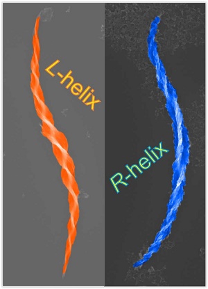
Twisted Semiconductors for Future Moving Holograms
March 30, 2017 | University of MichiganEstimated reading time: 3 minutes
A smartphone display that can produce moving, holographic 3D images will need to be able to twist the light it emits. Now, researchers at the University of Michigan and Ben-Gurion University of the Negev have discovered a way to mass produce spiral semiconductors that can take that important, light-coiling step.
Researchers at U-M unveiled some of the first holographic images in 1962, made by coaxing waves of light to form an array of bright and dark spots in space. This creates a static illusion of a material object. To make these frozen waves, researchers encoded images onto a material that could control the direction (polarization) and timing (phase) of the fluctuations within the electromagnetic waves.
The new semiconductor helices created by the U-M-led team offer that level of control over light in a format that could work in the pixels of displays. They can be incorporated into other semiconductor devices to vary the polarization, phase and color of light emitted by the different pixels, each of them made from the precisely designed semiconductor helices. This could one day enable moving holograms, projected by smartphones and other screens.
Until now, making semiconductors spirals with sufficiently strong twist—reminiscent of nanoscale fusilli pasta—was a difficult prospect because the twisted state is unnatural to semiconductor materials. They usually form sheets or wires. But Nicholas Kotov, the Joseph B. and Florence V. Cejka Professor of Chemical Engineering, and his team have found a way to guide the attachment of small semiconductor nanoparticles to each other with help from some of nature's twisted structures: proteins and DNA.
Amino acids are the quintessential building blocks of proteins," said Wenchun Feng, a postdoctoral research fellow in Kotov's lab and lead author of a newly published paper on the work. "The direction of the spiral of proteins is determined by the geometrical property of amino acids. We found that a common amino acid, cysteine, working together in large numbers, can twist not only proteins but also semiconductors."
The team coated nanoparticles made out of cadmium telluride, a semiconductor capable of emitting light, with cysteine. Cysteine comes in two forms that are mirror images of one another like our hands are, so it is known as a "chiral" molecule. They observed the nanoparticles spontaneously self-assembling into semiconductor "tornadoes" following the rightward or leftward chirality of the amino acid.
The team was surprised by the high fidelity of this self-assembly process and the strength of the twist. Nearly all—98 percent—of semiconductor helices had the same twisting direction and indeed looked like nanoscale fusilli. Some organic molecules can form natural spirals, too, but the light-twisting ability of semiconductor helices made by Kotov and colleagues is at least five times stronger.
When they shone light through the semiconductors, they recorded the photons swirling through them. Through a combination of experiments and computer simulations, the researchers developed design principles and methods for engineering the optical properties of the semiconductor helices for the different colors in future holography devices.
One of the unexpected consequences of this technology-driven project was getting a peek into mysteries surrounding how life may have arisen on Earth and why many biological molecules reliably follow either a clockwise or counterclockwise spiral. Kotov suggests that amino acids, which are known to form spontaneously in space dust, may have assembled nanoparticles into spirals that twisted the light from the early stars, serving as stable inorganic templates for organic molecules and particles to follow the same pattern.
The work is described in a study in Science Advances titled, "Assembly of mesoscale helices with near-unity enantiomeric excess and light-matter interactions for chiral semiconductors."
Share on:


Testimonial
"In a year when every marketing dollar mattered, I chose to keep I-Connect007 in our 2025 plan. Their commitment to high-quality, insightful content aligns with Koh Young’s values and helps readers navigate a changing industry. "
Brent Fischthal - Koh YoungSuggested Items
Curing and Verification in PCB Shadow Areas
09/17/2025 | Doug Katze, DymaxDesign engineers know a simple truth that often complicates electronics manufacturing: Light doesn’t go around corners. In densely populated PCBs, adhesives and coatings often fail to fully cure in shadowed regions created by tall ICs, connectors, relays, and tight housings.
VIDEOTON EAS's Bulgarian Subsidiary Expands Into Automotive Products
09/15/2025 | VideotonVEAS Bulgaria, engaged in electronics manufacturing, has joined the ranks of VIDEOTON companies authorized to produce automotive products.
Dymax Mexico to Showcase Light-Curing Technologies at SMTA Guadalajara Expo & Tech Forum 2025
09/05/2025 | DymaxDymax, a global manufacturer of rapid light-curing materials and equipment, will participate in SMTA Guadalajara Expo & Tech Forum, taking place September 17-18, 2025, at the Guadalajara Expo Center in Guadalajara, Jalisco, Mexico.
September 2025 SMT007 Magazine: An Eye on India
09/02/2025 | I-Connect007 Editorial TeamIndia is on track to become the world’s fastest-growing major economy within the next two years, and that momentum is already reshaping its electronics manufacturing sector. Whether you work with Indian suppliers or serve Indian customers, chances are the country will become a bigger part of your supply chain in the near future.
AiM Future, Franklin Wireless Sign MOU to Jointly Develop Lightweight AI Model and High-Efficiency 1 TOPS AI SoC Chipset
09/01/2025 | BUSINESS WIREAiM Future, a leading AI semiconductor design company, has signed a Memorandum of Understanding (MOU) with Franklin Wireless Corp., a global leader in intelligent wireless solutions, to jointly develop a lightweight AI model and a high-efficiency 1 TOPS performance AI SoC chipset.