


 The Marketing Minute: Cracking the Code of Technical Marketing
 Trouble in Your Tank: Implementing Direct Metallization in Advanced Substrate Packaging


Tiny Black Holes Enable a New Type of Photodetector for High-Speed Data
April 5, 2017 | UC DavisEstimated reading time: 2 minutes
Tiny “black holes” on a silicon wafer make for a new type of photodetector that could move more data at lower cost around the world or across a data center. The technology, developed by electrical engineers at the University of California, Davis, and W&WSens Devices Inc. of Los Altos, California, a Silicon Valley startup, is described in a paper published April 3 in the journal Nature Photonics.
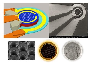
Tapered black holes in silicon, about 1 micrometer in size, can trap photons and act as a photodetector for high-speed data connections. (Saif Islam, UC Davis)
“We’re trying to take advantage of silicon for something silicon cannot usually do,” said Saif Islam, professor of electrical and computer engineering at UC Davis, who co-led the project together with the collaborators at W&WSens Devices Inc. Existing high-speed photodetector devices use materials such as gallium arsenide. “If we don’t need to add nonsilicon components and can monolithically integrate with electronics into a single silicon chip, the receivers become much cheaper.”
The new detector uses tapered holes in a silicon wafer to divert photons sideways, preserving the speed of thin-layer silicon and the efficiency of a thicker layer. So far, Islam’s group has built an experimental photodetector and solar cell using the new technology. The photodetector can convert data from optical to electronics at 20 gigabytes per second (or 25 billion bits per second, more than 200 times faster than your cable modem) with a quantum efficiency of 50 percent, the fastest yet reported for a device of this efficiency.
Data centers need fast connections
The growth of data centers that power the internet “cloud” has created a demand for devices to move large amounts of data, very fast, over short distances of a few yards to hundreds of yards. Such connections could also be used for high-speed home connections, Islam said.
When computer engineers want to move large amounts of data very fast, whether across the world or across a data center, they use fiber-optic cables that transmit data as pulses of light. But these signals need to be converted to electronic pulses at the receiving end by a photodetector. You can use silicon as a photodetector — incoming photons generate a flow of electrons. But there’s a tradeoff between speed and efficiency. To capture most of the photons, the piece of silicon needs to be thick, and that makes it relatively slow. Make the silicon thinner so it works faster, and too many photons get lost.
Instead, circuit designers have used materials such as gallium arsenide and indium phosphide to make high-speed, high-efficiency photodetectors. Gallium arsenide, for example, is about 10 times as efficient as a silicon at the same scale and wavelength. But it is significantly more expensive and cannot be monolithically integrated with silicon electronics.
Tapered holes as light traps
Islam’s group began by experimenting with ways to increase the efficiency of silicon by adding tiny pillars or columns, then holes to the silicon wafer. After two years of experiments, they settled on a pattern of holes that taper toward the bottom.“We came up with a technology that bends the incoming light laterally through thin silicon,” Islam said.The idea is that photons enter the holes and get pulled sideways into the silicon. The wafer itself is about 2 microns thick, but because they move sideways, the photons travel through 30 to 40 microns of silicon, like the ripple of waves on a pond when a pebble is dropped into the water.
The holes-based device can also potentially work with a wider range of wavelengths of light than current technology, Islam said.
Share on:


Testimonial
"We’re proud to call I-Connect007 a trusted partner. Their innovative approach and industry insight made our podcast collaboration a success by connecting us with the right audience and delivering real results."
Julia McCaffrey - NCAB GroupSuggested Items
Blaize, Technology Control Company Partner to Power Saudi Arabia’s Next-Generation AI Innovation Infrastructure
09/17/2025 | BUSINESS WIREBlaize Holdings, Inc., a leader in programmable, energy-efficient edge AI computing, and Technology Control Company (TCC), a leading technology solutions provider in the Kingdom of Saudi Arabia (KSA), announced a strategic partnership to advance Saudi Arabia’s AI innovation infrastructure and accelerate its digital transformation goals.
BLT Joins Microchip Partner Program as Design Partner
09/17/2025 | BUSINESS WIREBLT, a U.S.-owned and operated engineering design services firm announced it has joined the Microchip Design Partner Program.
Curing and Verification in PCB Shadow Areas
09/17/2025 | Doug Katze, DymaxDesign engineers know a simple truth that often complicates electronics manufacturing: Light doesn’t go around corners. In densely populated PCBs, adhesives and coatings often fail to fully cure in shadowed regions created by tall ICs, connectors, relays, and tight housings.
On the Line With… Podcast: UHDI and RF Performance
09/17/2025 | I-Connect007I-Connect007 is excited to announce the release of a new episode in its latest On the Line with... podcast series, which shines a spotlight on one of the most important emerging innovations in electronics manufacturing: Ultra-High-Density Interconnect (UHDI).
Altair, Wichita State University’s NIAR Sign MoU to Accelerate Aerospace Innovation
09/16/2025 | AltairAltair, a global leader in computational intelligence, and Wichita State University’s (WSU) National Institute for Aviation Research (NIAR), one of the world’s leading aerospace research institutions, have signed a memorandum of understanding (MoU) to advance innovation across the aerospace and defense industries.