


 The Marketing Minute: Cracking the Code of Technical Marketing
 Trouble in Your Tank: Implementing Direct Metallization in Advanced Substrate Packaging


Crystalline Material Could Replace Silicon to Double Efficiency of Solar Cells
April 7, 2017 | Purdue UniversityEstimated reading time: 3 minutes
A new material has been shown to have the capability to double the efficiency of solar cells by researchers at Purdue University and the National Renewable Energy Laboratory.
Conventional solar cells are at most one-third efficient, a limit known to scientists as the Shockley-Queisser Limit. The new material, a crystalline structure that contains both inorganic materials (iodine and lead) and an organic material (methyl-ammonium), boosts the efficiency so that it can carry two-thirds of the energy from light without losing as much energy to heat.
In less technical terms, this material could double the amount of electricity produced without a significant cost increase.
Enough solar energy reaches the earth to supply all of the planet's energy needs multiple times over, but capturing that energy has been difficult – as of 2013, only about 1 percent of the world's grid electricity was produced from solar panels.
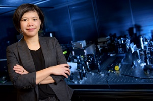
Libai Huang, assistant professor of chemistry at Purdue, says the new material, called a hybrid perovskites, would create solar cells thinner than conventional silicon solar cells, and is also flexible, cheap and easy to make.
"My graduate students learn how to make it in a few days," she says.
The breakthrough is published this week in the journal Science.
The most common solar cells use silicon as a semiconductor, which can transmit only one-third of the energy because of the band gap, which is the amount of energy needed to boost an electron from a bound state to a conducting state, in which the electrons are able to move, creating electricity.
Scientists at Purdue University and the National Renewable Energy Laboratory have discovered how electrons move in a new crystalline material and this discovery could lead to doubling the efficiency of solar cells. Ultrafast microscope images, such as these, show that the electrons in material is able to move over 200 nanometers with minimal energy loss to heat. (Purdue University image by Libai Huang)
Incoming photons can have more energy than the band gap, and for a very short time – so short it's difficult to imagine – the electrons exist with extra energy. These electrons are called "hot carriers," and in silicon they exist for only one picosecond (which is 10-12 seconds) and only travel a maximum distance of 10 nanometers. At this point the hot carrier electrons give up their energy as heat. This is one of the main reasons for the inefficiency of solar cells.
Huang and her colleagues have developed a new technique that can track the range of the motion and the speed of the hot carriers by using fast lasers and microscopes.
"The distance hot carriers need to migrate is at least the thickness of a solar cell, or about 200 nanometers, which this new perovskite material can achieve," Huang says. "Also these carriers can live for about 100 picoseconds, two orders of magnitude longer than silicon."
Kai Zhu, senior scientist at the National Renewable Energy Laboratory in Golden, Colorado, and one of the journal paper’s co-authors, says that these are critical factors for creating a commercial hot-carrier solar cell.
The potential to double the efficiency of solar cells using a new unique material has been discovered by Purdue University and the National Renewable Energy Laboratory. The material, called a hybrid perovskite, has an inorganic crystal "cage" which contains an organic molecule, methyl-ammonium. (Purdue University image by Libai Huang)
"This study demonstrated that hot carriers in a standard polycrystalline perovskite thin film can travel for a distance that is similar to or longer than the film thickness required to build an efficient perovskite solar cell," he says. "This indicates that the potential for developing hot carrier perovskite solar cell is good."
However, before a commercial product is developed, researchers are trying to use the same techniques developed at Purdue by replacing lead in the material with other, less toxic, metals.
"The next step is to find or develop suitable contact materials or structures with proper energy levels to extract these hot carriers to generate power in the external circuit," Zhu says. "This may not be easy."
Huang's research at Purdue was funded by National Science Foundation grant DMR- 1507803.
The work at the National Renewable Energy Laboratory was funded by the Solar Energy Technologies Office of the U.S. Department of Energy's Office of Energy Efficiency and Renewable Energy.
Share on:


Testimonial
"We’re proud to call I-Connect007 a trusted partner. Their innovative approach and industry insight made our podcast collaboration a success by connecting us with the right audience and delivering real results."
Julia McCaffrey - NCAB GroupSuggested Items
Rules of Thumb: Design007 Magazine, November 2024
11/11/2024 | I-Connect007 Editorial TeamRules of thumb are everywhere, but there may be hundreds of rules of thumb for PCB design. They’re built on design formulas, fabricators’ limitations, and tribal knowledge. And unfortunately, some longtime rules of thumb should be avoided at all costs. How do we separate the wheat from the chaff, so to speak?
Connect the Dots: Best Practices for Prototyping
09/21/2023 | Matt Stevenson -- Column: Connect the DotsPCB prototyping is a critical juncture during an electronic device’s journey from concept to reality. Regardless of a project’s complexity, the process of transforming a design into a working board is often enlightening in terms of how a design can be improved before a PCB is ready for full production.
The Drive Toward UHDI and Substrates
09/20/2023 | I-Connect007 Editorial TeamPanasonic’s Darren Hitchcock spoke with the I-Connect007 Editorial Team on the complexities of moving toward ultra HDI manufacturing. As we learn in this conversation, the number of shifting constraints relative to traditional PCB fabrication is quite large and can sometimes conflict with each other.
Asia/Pacific AI Spending Surge to Reach a Projected $78 Billion by 2027
09/19/2023 | IDCAsia/Pacific spending on Artificial Intelligence (AI) ), including software, services, and hardware for AI-centric systems will grow to $78.4 billion in 2027, according to International Data Corporation's latest Worldwide Artificial Intelligence Spending Guide.
Intel to Sell Minority Stake in IMS Nanofabrication Business to TSMC
09/13/2023 | IntelIntel Corporation announced that it has agreed to sell an approximately 10% stake in the IMS Nanofabrication business to TSMC. TSMC’s investment values IMS at approximately $4.3 billion, consistent with the valuation of the recent stake sale to Bain Capital Special Situations.