


 The Marketing Minute: Cracking the Code of Technical Marketing
 Trouble in Your Tank: Implementing Direct Metallization in Advanced Substrate Packaging


Green IT: New Switching Process in Non-volatile Spintronics Devices
April 20, 2017 | HZBEstimated reading time: 2 minutes
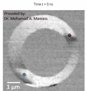
Physicists achieved a robust and reliable magnetization switching process by domain wall displacement without any applied fields. The effect is observed in tiny asymmetric permalloy rings and may pave the way to extremely efficient new memory devices. The results have been published in Physical Review Applied, highlighted as an Editors' Suggestion.
To construct magnetic memories, elements with two stable magnetization states are needed. Promising candidate for such magnetic elements are tiny rings, typically of the order of few micrometers, with clockwise or counterclockwise magnetization as the two states. Unfortunately, switching between those two states directly requires a circular magnetic field which is not easy to achieve.
A magnetic field pulse switches the initial vortex state to “onion state” with two walls. In the subsequent magnetic snapshots the domain wall motion is shown. After 58 ns both walls meet and annihilate, thus completing the switching process into the opposite sense of rotation. Credit: HZB
Switching in asymmetric nanorings
But this problem can be solved, as demonstrated by a team of scientists from several institutions in Germany including Helmholtz-Zentrum Berlin: If the hole in the ring is slightly displaced, thus making the ring thinner on one side, a simple, uniaxial magnetic field pulse of some nanoseconds duration can switches between the two possible “vortex states” used for data storage (clockwise and counterclockwise).
Short magnetic field pulse is sufficient
The scientists recorded the time evolution of the magnetization dynamics of the device at the Maxymus-Beamline at BESSY II employing time-resolved x-ray microscopy during and after the short magnetic field pulse was applied. They observed how the magnetic field pulse leads in a first step to an intermediate “onion state” in the ring. This state is characterized by two domain walls, where different magnetization zones meet each other. After the external field pulse has vanished, these domain walls move towards each other and annihilate, which results in a stable opposite magnetization of the ring “vortex state”.
Very fast process for spintronics
“Our measurements show domain wall automotion with an average velocity of about 60 m/s. This is very fast for spintronic devices at zero applied field”, Dr. Mohamad-Assaad Mawass, lead author of the publication in Physical Review Applied, points out. Mawass has worked on these experiments already for his PhD at Johannes Gutenberg University Mainz (group of Prof. Kläui) in a joined project with Max Planck Institute for intelligent system at Stuttgart (Schütz-Department). He then continued his research as a postdoc research Scientist at X-PEEM beamline at HZB.
Details of domain wall motion observed
Another observation concerns the effect of the detailed topological nature of the walls in the annihilation process. According to the results, this effect influence the dynamics only on a local scale where walls experience an attractive or repulsive interaction once they get very close to each other without inhibiting the annihilation of walls through automotion. “The domain wall inertia and the stored energy, in the system, allows the walls to overcome both the local extrinsic pinning and the topological repulsion between DWs carrying the same winding number” said Mawass. “We believe to have identified a robust and reliable switching process by domain wall automotion in ferromagnetic rings”, Mawass states. “This could pave the way for further optimization of these devices.”
Share on:


Testimonial
"Advertising in PCB007 Magazine has been a great way to showcase our bare board testers to the right audience. The I-Connect007 team makes the process smooth and professional. We’re proud to be featured in such a trusted publication."
Klaus Koziol - atgSuggested Items
Alternative Manufacturing, Inc. (AMI) Announces Commitment to Excellence in Industrial, Defense, Aerospace, Renewables, and Robotics Markets
09/16/2025 | Alternative Manufacturing, Inc.Alternative Manufacturing, Inc. (AMI), a 100% employee-owned contract manufacturer, proudly reaffirms its leadership in the electronics manufacturing services (EMS) industry with a continued commitment to delivering high-quality PCBAs and box builds across the industrial, defense, aerospace, renewable energy, and robotics markets.
Sustainability and Selective Soldering
09/15/2025 | Dr. Samuel J. McMaster, Pillarhouse InternationalSustainability is more than just a buzzword for the electronics industry; it’s a key goal for all manufacturing processes. This is more than a box-ticking exercise or simply doing a small part for environmentally friendly processes. Moving toward sustainable solutions drives innovation and operational efficiency.
Trouble in Your Tank: Implementing Direct Metallization in Advanced Substrate Packaging
09/15/2025 | Michael Carano -- Column: Trouble in Your TankDirect metallization systems based on conductive graphite are gaining popularity throughout the world. The environmental and productivity gains achievable with this process are outstanding. Direct metallization reduces the costs of compliance, waste treatment, and legal issues related to chemical exposure. A graphite-based direct plate system has been devised to address these needs.
EV Group Achieves Breakthrough in Hybrid Bonding Overlay Control for Chiplet Integration
09/12/2025 | EV GroupEV Group (EVG), a leading provider of innovative process solutions and expertise serving leading-edge and future semiconductor designs and chip integration schemes, today unveiled the EVG®40 D2W—the first dedicated die-to-wafer overlay metrology platform to deliver 100 percent die overlay measurement on 300-mm wafers at high precision and speeds needed for production environments. With up to 15X higher throughput than EVG’s industry benchmark EVG®40 NT2 system designed for hybrid wafer bonding metrology, the new EVG40 D2W enables chipmakers to verify die placement accuracy and take rapid corrective action, improving process control and yield in high-volume manufacturing (HVM).
Integrating Uniplate PLBCu6 With the Digital Factory Suite
09/12/2025 | Giovanni Obino and Andreas Schatz, MKS' AtotechPrinted circuit board manufacturing is rapidly changing, driven by miniaturization, stringent reliability requirements, and growing pressure for sustainable production. Meeting these challenges requires more than incremental improvements; it demands a combination of precise equipment and real-time process intelligence. The pairing of Uniplate® PLBCu6 with the Digital Factory Suite (DFS) demonstrates how hardware and software can work together to create more responsive, resource-efficient manufacturing.