


 The Marketing Minute: Cracking the Code of Technical Marketing
 Trouble in Your Tank: Implementing Direct Metallization in Advanced Substrate Packaging


Single-Molecule Diode Created
April 27, 2017 | Universitat de BarcelonaEstimated reading time: 1 minute
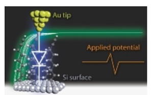
Researchers of the University of Barcelona have led a project to create a diode out of a 1 nm-sized single molecule with high rectification ratios. Diodes, commonly used in in everyday electronic devices, allow current to flow in one direction while blocking the current in the opposite direction.
Today, researchers are approaching the physical limit in downsizing electronic components. According to Ismael Díez Pérez, who is leading the project at the University of Barcelona and is also member of the Institute of Bioengineering of Catalonia (IBEC), “In order to go to the next level of miniaturization, we have to use individual molecules as the active components of the circuits“. This study, recently published in the journal Nature Communications, has used an organic molecule sandwiched between two nano-electrodes connected altogether in a circuit that is barely 1 nm long. The resulting single-molecule diode is smaller and much more efficient than any other reported. “This approach favours the assembly of thousands of billions of diodes on a tiny silicon chip”, affirms Díez-Pérez.
The reported molecular diode can allow current to go in one direction 4.000 times more than in the opposite direction. This efficiency is comparable to the diodes that are currently used, which are much bigger.
The team is now working on achieving higher current rectification ratios and increasing the lifetime of these single-molecule circuits. This research brings us a step closer to the realisation of single-molecule devices.
Share on:


Testimonial
"Our marketing partnership with I-Connect007 is already delivering. Just a day after our press release went live, we received a direct inquiry about our updated products!"
Rachael Temple - AlltematedSuggested Items
U.S. Uses Secret Trackers to Trace AI Chips Diverted to China, Sources Say
08/18/2025 | I-Connect007 Editorial TeamTwo sources told Reuters that U.S. authorities have secretly placed location trackers in some advanced chip shipments they see as at high risk of illegal diversion to China. They said the trackers are intended to locate AI chips that are sent to locations restricted by U.S. export laws, but authorities only examine some shipments.
Happy’s Tech Talk #38: Novel Metallization for UHDI
05/07/2025 | Happy Holden -- Column: Happy’s Tech TalkI have been involved in high-density electronics substrates since 1970 when I joined Hewlett-Packard’s RF semiconductor group after college. Figure 1 shows the difference between trace/space lithography for substrates and silicon starting in 1970. My projects involved sapphire circuits for RF devices, but the figure displays the state of PCBs and integrated CMOS circuits and their packaging, not discreet RF devices. Even then, semiconductors were 50X higher density.
New Database of Materials Accelerates Electronics Innovation
05/05/2025 | ACN NewswireIn a collaboration between Murata Manufacturing Co., Ltd., and the National Institute for Materials Science (NIMS), researchers have built a comprehensive new database of dielectric material properties curated from thousands of scientific papers.
New Database of Materials Accelerates Electronics Innovation
05/02/2025 | ACN NewswireIn a collaboration between Murata Manufacturing Co., Ltd., and the National Institute for Materials Science (NIMS), researchers have built a comprehensive new database of dielectric material properties curated from thousands of scientific papers.
Micron Announces Business Unit Reorganization to Capitalize on AI Growth Across All Market Segments
04/23/2025 | MicronMicron Technology, Inc., a leader in innovative memory and storage solutions, announced a market segment-based reorganization of its business units to capitalize on the transformative growth driven by AI, from data centers to edge devices.