


 The Marketing Minute: Cracking the Code of Technical Marketing
 Trouble in Your Tank: Implementing Direct Metallization in Advanced Substrate Packaging


'Persistent Photoconductivity' Offers New Tool for Bioelectronics
May 3, 2017 | NC State UniversityEstimated reading time: 1 minute
Researchers at North Carolina State University have developed a new approach for manipulating the behavior of cells on semiconductor materials, using light to alter the conductivity of the material itself.
“There’s a great deal of interest in being able to control cell behavior in relation to semiconductors – that’s the underlying idea behind bioelectronics,” says Albena Ivanisevic, a professor of materials science and engineering at NC State and corresponding author of a paper on the work. “Our work here effectively adds another tool to the toolbox for the development of new bioelectronic devices.”
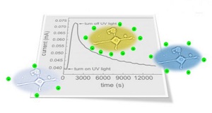
The new approach makes use of a phenomenon called persistent photoconductivity. Materials that exhibit persistent photoconductivity become much more conductive when you shine a light on them. When the light is removed, it takes the material a long time to return to its original conductivity.
When conductivity is elevated, the charge at the surface of the material increases. And that increased surface charge can be used to direct cells to adhere to the surface.
“This is only one way to control the adhesion of cells to the surface of a material,” Ivanisevic says. “But it can be used in conjunction with others, such as engineering the roughness of the material’s surface or chemically modifying the material.”
For this study, the researchers demonstrated that all three characteristics can be used together, working with a gallium nitride substrate and PC12 cells – a line of model cells used widely in bioelectronics testing.
The researchers tested two groups of gallium nitride substrates that were identical, except that one group was exposed to UV light – triggering its persistent photoconductivity properties – while the second group was not.
“There was a clear, quantitative difference between the two groups – more cells adhered to the materials that had been exposed to light,” Ivanisevic says.
“This is a proof-of-concept paper,” Ivanisevic says. “We now need to explore how to engineer the topography and thickness of the semiconductor material in order to influence the persistent photoconductivity and roughness of the material. Ultimately, we want to provide better control of cell adhesion and behavior.”
Share on:


Testimonial
"We’re proud to call I-Connect007 a trusted partner. Their innovative approach and industry insight made our podcast collaboration a success by connecting us with the right audience and delivering real results."
Julia McCaffrey - NCAB GroupSuggested Items
Curing and Verification in PCB Shadow Areas
09/17/2025 | Doug Katze, DymaxDesign engineers know a simple truth that often complicates electronics manufacturing: Light doesn’t go around corners. In densely populated PCBs, adhesives and coatings often fail to fully cure in shadowed regions created by tall ICs, connectors, relays, and tight housings.
Marcy’s Musings: Advancing the Advanced Materials Discussion
09/17/2025 | Marcy LaRont -- Column: Marcy's MusingsAs the industry’s most trusted global source of original content about the electronics supply chain, we continually ask you about your concerns, what you care about, and what you most want to learn about. Your responses are insightful and valuable. Thank you for caring enough to provide useful feedback and engage in dialogue.
September 2025 PCB007 Magazine: The Future of Advanced Materials
09/16/2025 | I-Connect007 Editorial TeamMoore’s Law is no more, and the advanced material solutions being developed to grapple with this reality are surprising, stunning, and perhaps a bit daunting. Buckle up for a dive into advanced materials and a glimpse into the next chapters of electronics manufacturing.
I-Connect007 Launches Advanced Electronics Packaging Digest
09/15/2025 | I-Connect007I-Connect007 is pleased to announce the launch of Advanced Electronics Packaging Digest (AEPD), a new monthly digital newsletter dedicated to one of the most critical and rapidly evolving areas of electronics manufacturing: advanced packaging at the interconnect level.
Panasonic Industry will Double the Production Capacity of MEGTRON Multi-layer Circuit Board Materials Over the Next Five Years
09/15/2025 | Panasonic Industry Co., Ltd.Panasonic Industry Co., Ltd., a Panasonic Group company, announced plans for a major expansion of its global production capacity for MEGTRON multi-layer circuit board materials today. The company plans to double its production over the next five years to meet growing demand in the AI server and ICT infrastructure markets.