


 The Marketing Minute: Cracking the Code of Technical Marketing
 Trouble in Your Tank: Implementing Direct Metallization in Advanced Substrate Packaging


Wafer-thin Magnetic Materials Developed for Future Quantum Technologies
May 22, 2017 | University of BaselEstimated reading time: 2 minutes
Two-dimensional magnetic structures are regarded as a promising material for new types of data storage, since the magnetic properties of individual molecular building blocks can be investigated and modified. For the first time, researchers have now produced a wafer-thin ferrimagnet, in which molecules with different magnetic centers arrange themselves on a gold surface to form a checkerboard pattern. Scientists at the Swiss Nanoscience Institute at the University of Basel and the Paul Scherrer Institute published their findings in the journal Nature Communications.
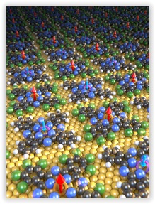
Phthalocyanines with iron (orange) and manganese (violet) centers co-assemble on a gold surface into a checkerboard pattern. The magnetism of iron and manganese differs in strength and points in opposite directions (red and blue arrows), fulfilling the prerequisites for extremely, atomically thin ferrimagnets. (Image: University of Basel, Department of Physics)
Ferrimagnets are composed of two centers which are magnetized at different strengths and point in opposing directions. Two-dimensional, quasi-flat ferrimagnets would be suitable for use as sensors, data storage devices or in a quantum computer, since the two-dimensional arrangement allows the magnification state of the individual atoms or molecules to be selected. For mathematical and geometrical reasons, however, it has so far not been possible to produce two-dimensional ferrimagnets.
Choice of materials makes the impossible possible
The scientists in Professor Thomas Jung’s research groups at the Paul Scherrer Institute (PSI) and the Department of Physics at the University of Basel have now found a method of making a two-dimensional ferrimagnet.
The researchers first produce “phthalocyanines” – hydrocarbon compounds with different magnetic centers composed of iron and manganese. When these phthalocyanines are applied to a gold surface, they arrange themselves into a checkerboard pattern in which molecules with iron and manganese centers alternate. The researchers were able to prove that the surface is magnetic, and that the magnetism of the iron and manganese is of different strengths and appears in opposing directions – all characteristics of a ferrimagnet.
“The decisive factor of this discovery is the electrically conductive gold substrate, which mediates the magnetic order,” explains Dr. Jan Girovsky from the PSI, lead author of the study. “Without the gold substrate, the magnetic atoms would not sense each other and the material would not be magnetic.”
The decisive effect of the conducting electrons in the gold substrate is shown by a physical effect detected in each magnetic atom using scanning tunnel spectroscopy. The experiments were conducted at various temperatures and thus provide evidence of the strength of the magnetic coupling in the new magnetic material. Model calculations confirmed the experimentally observed effect and indicated that special electrons attached to the surface in the gold substrate are responsible for this type of magnetism.
Nanoarchitecture leads to new magnetic materials
“The work shows that a clever combination of materials and a particular nanoarchitecture can be used to produce new materials that otherwise would be impossible,” says Professor Nirmalya Ballav of the Indian Institute of Science Education and Research in Pune (India), who has been studying the properties of molecular nano-checkerboard architectures for several years with Jung. The magnetic molecules have great potential for a number of applications, since their magnetism can be individually investigated and also modified using scanning tunnel spectroscopy.
Original source
Jan Girovsky, Jan Nowakowski, Md. Ehesan Ali, Milos Baljozovic, Harald R. Rossmann, Thomas Nijs, Elise A. Aeby, Sylwia Nowakowska, Dorota Siewert, Gitika Srivastava, Christian Wackerlin, Jan Dreiser, Silvio Decurtins, Shi-Xia Liu, Peter M. Oppeneer, Thomas A. Jung and Nirmalya Ballav
Share on:


Testimonial
"We’re proud to call I-Connect007 a trusted partner. Their innovative approach and industry insight made our podcast collaboration a success by connecting us with the right audience and delivering real results."
Julia McCaffrey - NCAB GroupSuggested Items
Driving Innovation: Depth Routing Processes—Achieving Unparalleled Precision in Complex PCBs
09/08/2025 | Kurt Palmer -- Column: Driving InnovationIn PCB manufacturing, the demand for increasingly complex and miniaturized designs continually pushes the boundaries of traditional fabrication methods, including depth routing. Success in these applications demands not only on robust machinery but also sophisticated control functions. PCB manufacturers rely on advanced machine features and process methodologies to meet their precise depth routing goals. Here, I’ll explore some crucial functions that empower manufacturers to master complex depth routing challenges.
Polar Instruments Announces Additive Transmission Line Support for Si9000e
08/20/2025 | Polar InstrumentsTransmission lines embedded into the PCB surface are a feature of UHDI constructions. The 2025 fall release of Polar's Si9000e PCB impedance & insertion loss transmission line field solver incorporates eight new single ended, differential and coplanar transmission line structures.
Henniker Plasma Launches Stratus Turnkey Plasma Manufacturing Cell
08/13/2025 | Henniker PlasmaHenniker Plasma, a leading manufacturer of plasma treatment systems, proudly announces the launch of its Stratus Plasma Manufacturing Cell range — a fully integrated, turnkey solution that combines advanced atmospheric plasma surface treatment with robotic automation.
Trouble in Your Tank: Metallizing Flexible Circuit Materials—Mitigating Deposit Stress
08/04/2025 | Michael Carano -- Column: Trouble in Your TankMetallizing materials, such as polyimide used for flexible circuitry and high-reliability multilayer printed wiring boards, provide a significant challenge for process engineers. Conventional electroless copper systems often require pre-treatments with hazardous chemicals or have a small process window to achieve uniform coverage without blistering. It all boils down to enhancing the adhesion of the thin film of electroless copper to these smooth surfaces.
Designers Notebook: Basic PCB Planning Criteria—Establishing Design Constraints
07/22/2025 | Vern Solberg -- Column: Designer's NotebookPrinted circuit board development flows more smoothly when all critical issues are predefined and understood from the start. As a basic planning strategy, the designer must first consider the product performance criteria, then determine the specific industry standards or specifications that the product must meet. Planning also includes a review of all significant issues that may affect the product’s manufacture, performance, reliability, overall quality, and safety.