


 The Marketing Minute: Cracking the Code of Technical Marketing
 Trouble in Your Tank: Implementing Direct Metallization in Advanced Substrate Packaging


Unexpected Property May Raise Material’s Prospects as Solar Cell
May 23, 2017 | NISTEstimated reading time: 4 minutes
Crystalline materials known as perovskites could become the next superstars of solar cells. Over the past few years, researchers have demonstrated that a special class of perovskites—those consisting of a hybrid of organic and inorganic components—convert sunlight into electricity with an efficiency above 20 percent and are easier to fabricate and more impervious to defects than the standard solar cell made of crystalline silicon. As fabricated today, however, these organic/inorganic perovskites (OIPs) deteriorate well before the typical 30-year lifetime for silicon cells, which prevents their widespread use in harnessing solar power.
Now a team led by Andrea Centrone at the National Institute of Standards and Technology (NIST) and Jinsong Huang and Alexei Gruverman of the University of Nebraska has found the first solid evidence for a property of OIPs that may provide a new way to improve their long-term stability as solar cells.
The unexpected feature that the team found is known as ferroelasticity—a spontaneous rearrangement of the internal structure of OIPs in which each crystal subdivides into a series of tiny regions, or domains, that have the same atomic arrangement but which are oriented in different directions. This rearrangement creates a spontaneous strain in each domain that exists even in the absence of any external stress (force).
“The role of the ferroelastic domains on the material stability must be understood,” said Centrone.
At high temperatures, OIP crystals do not subdivide and have the same cubic arrangement of atoms throughout. At room temperature, however, the OIP crystal structure changes from cubic to tetragonal, in which one axis of the cube elongates. That’s where the ferroelastic property of the material comes into play.
“To transform from a cubic to a tetragonal arrangement, one axis of the cube must elongate. In the process, each crystal subdivides into smaller domains in which the elongated axis can point in a different direction, leading to spontaneous internal strain,” explained team member Evgheni Strelcov of NIST and the University of Maryland.
At present, it remains unknown whether ferroelasticity is a property that improves or hinders the performance and stability of perovskite solar cells, noted Centrone. But the very fact that OIPs have this internal structure, breaking up single crystals into domains, is important to investigate, he added. Boundaries between crystals—so-called inter-grain boundaries—are known to be weak points, where structural defects concentrate. Similarly, the boundaries between the newly discovered ferroelastic domains inside a single crystal—intra-grain boundaries—might also affect the stability of OIPs and their performance as solar cells.
Image recorded by an atomic force microscope reveals the topography of a polycrystalline sample of the perovskite, including the boundaries between crystals. Credit: NIST
Image taken with the photothermal induced resonance technique shows the newly discovered ferroelastic domains (striations) within most crystals. Scale shows the PTIR signal intensity, a measure of the infrared light absorbed by the sample. Credit: NIST
The researchers discovered that by bending the crystals, they could reliably move, create or eliminate the ferroelastic grain boundaries—the borders between subdivided crystal regions having different orientations—thus enlarging or reducing the size of each domain. The bending also changed the relative fraction of domains pointing in different orientations. The researchers recently described their work (link is external) in Science Advances.
In their study, the team found no evidence that the OIPs were ferroelectric; in other words, that they formed domains where the separation of the center of positive and negative electric charges is aligned in different directions in the absence of an external electric field. This finding is significant, because some researchers had speculated that ferroelectricity might be the underlying property that makes OIPs promising candidates for solar cells.
The researchers created single whole crystals large enough to reveal ferroelastic domains, which appeared as striations with an optical microscope. They also studied OIPs consisting of polycrystalline thin films, which were examined using nanoscale techniques.
The researchers used two nanoscale methods employing atomic force microscope (AFM) probes to measure ferroelasticity in OIP thin films. At the University of Nebraska, Gruverman and his collaborators used piezoresponse force microscopy (PFM), which mapped the electrically induced mechanical response of an OIP sample in repose and under mechanical stress by gently bending the sample.
Illustration shows that in response to an applied stress, such as bending, the boundaries of the ferroelastic domains (red and blue regions depict domains oriented in different directions) become bigger or smaller. Credit: NIST
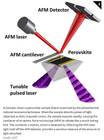
In the other method, laser pulses spanning from the visible to the infrared ranges struck a perovskite thin film, causing the material to heat up and expand. The tiny expansion was captured and amplified by the AFM probe using photothermal induced resonance (PTIR), a technique that combines the resolution of an AFM with the precise compositional information provided by infrared spectroscopy. PTIR imaging revealed the presence of microscopic striations that persisted even when the samples were subjected to heating or applied voltage. Experiments showed that the striations were not correlated with the local chemical composition or optical properties, but were due to differences in thermal expansion coefficient of the ferroelastic domains.
Share on:


Testimonial
"Our marketing partnership with I-Connect007 is already delivering. Just a day after our press release went live, we received a direct inquiry about our updated products!"
Rachael Temple - AlltematedSuggested Items
MEMS & Imaging Sensors Summit to Spotlight Sensing Revolution for Europe’s Leadership
09/11/2025 | SEMIIndustry experts will gather November 19-20 at the SEMI MEMS & Imaging Sensors Summit 2025 to explore the latest breakthroughs in AI-driven MEMS and imaging optimization, AR/VR technologies, and advanced sensor solutions for critical defence applications.
Direct Imaging System Market Size to Hit $4.30B by 2032, Driven by Increasing Demand for High-Precision PCB Manufacturing
09/11/2025 | Globe NewswireAccording to the SNS Insider, “The Direct Imaging System Market size was valued at $2.21 Billion in 2024 and is projected to reach $4.30 Billion by 2032, growing at a CAGR of 8.68% during 2025-2032.”
I-Connect007’s Editor’s Choice: Five Must-Reads for the Week
07/04/2025 | Marcy LaRont, I-Connect007For our industry, we have seen several bullish market announcements over the past few weeks, including one this week by IDC on the massive growth in the global server market. We’re also closely watching global trade and nearshoring. One good example of successful nearshoring is Rehm Thermal Systems, which celebrates its 10th anniversary in Mexico and the official opening of its new building in Guadalajara.
Driving Innovation: Direct Imaging vs. Conventional Exposure
07/01/2025 | Simon Khesin -- Column: Driving InnovationMy first camera used Kodak film. I even experimented with developing photos in the bathroom, though I usually dropped the film off at a Kodak center and received the prints two weeks later, only to discover that some images were out of focus or poorly framed. Today, every smartphone contains a high-quality camera capable of producing stunning images instantly.
United Electronics Corporation Advances Manufacturing Capabilities with Schmoll MDI-ST Imaging Equipment
06/24/2025 | United Electronics CorporationUnited Electronics Corporation has successfully installed the advanced Schmoll MDI-ST (XL) imaging equipment at their advanced printed circuit board facility. This significant technology investment represents a continued commitment to delivering superior products and maintaining their position as an industry leader in precision PCB manufacturing.