


 The Marketing Minute: Cracking the Code of Technical Marketing
 Trouble in Your Tank: Implementing Direct Metallization in Advanced Substrate Packaging


Researchers Find New Way to Control Light with Electric Fields
May 29, 2017 | NC State UniversityEstimated reading time: 2 minutes
Researchers from North Carolina State University have discovered a technique for controlling light with electric fields.
“Our method is similar to the technique used to provide the computing capabilities of computers,” says Linyou Cao, an assistant professor of materials science and engineering at NC State and corresponding author of a paper on the work. “In computers, an electric field is used to turn electric current on or off, which corresponds to logic 1 and logic 0, the basis of binary code. With this new discovery, a light may be controlled to be strong or weak, spread or focused, pointing one direction or others by an electric field. We think that, just as computers have changed our way of thinking, this new technique will likely change our way of watching. For instance, it may shape a light into arbitrary patterns, which may find applications in goggle-free virtual reality lenses and projectors, the animation movie industry or camouflage.”
Controlling light with electric fields is difficult. Photons, the basic units of light, are neutral – they have no charge, so they usually do not respond to electric fields. Instead, light may be controlled by tuning the refractive index of materials. Refractive index refers to the way materials reflect, transmit, scatter and absorb light. The more one can control a material’s refractive index, the more control you have over the light that interacts with that material.
“Unfortunately, it is very difficult to tune refractive index with electric fields,” Cao says. “Previous techniques could only change the index for visible light by between 0.1 and 1 percent at the maximum.”
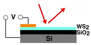
Cao and his collaborators have developed a technique that allows them to change the refractive index for visible light in some semiconductor materials by 60 percent – two orders of magnitude better than previous results. The researchers worked with a class of atomically thin semiconductor materials called transition metal dichalcogenide monolayers. Specifically, they worked with thin films of molybdenum sulfide, tungsten sulfide and tungsten selenide.
“We changed the refractive index by applying charge to two-dimensional semiconductor materials in the same way one would apply charge to transistors in a computer chip,” Cao says. “Using this technique, we achieved significant, tunable changes in the index within the red range of the visible spectrum.”
Currently, the new technique allows researchers to tune the refractive index by any amount up to 60 percent – the greater the voltage applied to the material, the greater the degree of change in the index. And, because the researchers are using the same techniques found in existing computational transistor technologies, these changes are dynamic and can be made billions of times per second.
“This technique may provide capabilities to control the amplitude and phase of light pixel by pixel in a way as fast as modern computers,” says Yiling Yu, a recent graduate of NC State and lead author of the paper.
“This is only a first step,” Cao says. “We think we can optimize the technique to achieve even larger changes in the refractive index. And we also plan to explore whether this could work at other wavelengths in the visual spectrum.”
Cao and his team are also looking for industry partners to develop new applications for the discovery.
Share on:


Testimonial
"In a year when every marketing dollar mattered, I chose to keep I-Connect007 in our 2025 plan. Their commitment to high-quality, insightful content aligns with Koh Young’s values and helps readers navigate a changing industry. "
Brent Fischthal - Koh YoungSuggested Items
Curing and Verification in PCB Shadow Areas
09/17/2025 | Doug Katze, DymaxDesign engineers know a simple truth that often complicates electronics manufacturing: Light doesn’t go around corners. In densely populated PCBs, adhesives and coatings often fail to fully cure in shadowed regions created by tall ICs, connectors, relays, and tight housings.
Marcy’s Musings: Advancing the Advanced Materials Discussion
09/17/2025 | Marcy LaRont -- Column: Marcy's MusingsAs the industry’s most trusted global source of original content about the electronics supply chain, we continually ask you about your concerns, what you care about, and what you most want to learn about. Your responses are insightful and valuable. Thank you for caring enough to provide useful feedback and engage in dialogue.
September 2025 PCB007 Magazine: The Future of Advanced Materials
09/16/2025 | I-Connect007 Editorial TeamMoore’s Law is no more, and the advanced material solutions being developed to grapple with this reality are surprising, stunning, and perhaps a bit daunting. Buckle up for a dive into advanced materials and a glimpse into the next chapters of electronics manufacturing.
I-Connect007 Launches Advanced Electronics Packaging Digest
09/15/2025 | I-Connect007I-Connect007 is pleased to announce the launch of Advanced Electronics Packaging Digest (AEPD), a new monthly digital newsletter dedicated to one of the most critical and rapidly evolving areas of electronics manufacturing: advanced packaging at the interconnect level.
Panasonic Industry will Double the Production Capacity of MEGTRON Multi-layer Circuit Board Materials Over the Next Five Years
09/15/2025 | Panasonic Industry Co., Ltd.Panasonic Industry Co., Ltd., a Panasonic Group company, announced plans for a major expansion of its global production capacity for MEGTRON multi-layer circuit board materials today. The company plans to double its production over the next five years to meet growing demand in the AI server and ICT infrastructure markets.