


 The Marketing Minute: Cracking the Code of Technical Marketing
 Trouble in Your Tank: Implementing Direct Metallization in Advanced Substrate Packaging


New Method of Characterizing Graphene
May 30, 2017 | University of BaselEstimated reading time: 2 minutes
Scientists have developed a new method of characterizing graphene’s properties without applying disruptive electrical contacts, allowing them to investigate both the resistance and quantum capacitance of graphene and other two-dimensional materials. Researchers from the Swiss Nanoscience Institute and the University of Basel’s Department of Physics reported their findings in the journal Physical Review Applied.
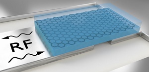
The layer of graphene (black honeycomb structure) encapsulated in boron nitride (blue) is placed on a superconductor (gray) and coupled with a microwave resonator. By comparing microwave signals (RF), the resistance and quantum capacitance of the embedded graphene can be determined. (Image: University of Basel, Department of Physics/Swiss Nanoscience Institute)
Graphene consists of a single layer of carbon atoms. It is transparent, harder than diamond and stronger than steel, yet flexible, and a significantly better conductor of electricity than copper. Since graphene was first isolated in 2004, scientists across the world have been researching its properties and the possible applications for the ultrathin material. Other two-dimensional materials with similarly promising fields of application also exist; however, little research has been carried out into their electronic structures.
No need for electrical contacts
Electrical contacts are usually used to characterize the electronic properties of graphene and other two-dimensional materials. However, these can significantly alter the materials’ properties. Professor Christian Schönenberger’s team from the Swiss Nanoscience Institute and the University of Basel’s Department of Physics has now developed a new method of investigating these properties without applying contacts.
To do this, the scientists embedded graphene in the isolator boron nitride, placed it on a superconductor and coupled it with a microwave resonator. Both the electrical resistance and the quantum capacitance of the graphene affect the quality factor and resonance frequency of the resonator. Although these signals are very weak, they can be captured using superconducting resonators.
By comparing the microwave characteristics of resonators with and without encapsulated graphene, the scientists can determine both the electrical resistance and quantum capacitance. “These parameters are important in the determination of graphene’s exact properties and in the identification of limiting factors for its application,” explains Simon Zihlmann, a PhD student in Schönenberger’s group.
Also suitable for other two-dimensional materials
The boron nitride-encapsulated graphene served as a prototype material during the method’s development. Graphene integrated into other materials can be investigated in the same way. In addition, other two-dimensional materials can also be characterized without the use of electrical contacts; for example, the semiconductor molybdenum disulfide, which has applications in solar cells and optics.
Share on:


Testimonial
"We’re proud to call I-Connect007 a trusted partner. Their innovative approach and industry insight made our podcast collaboration a success by connecting us with the right audience and delivering real results."
Julia McCaffrey - NCAB GroupSuggested Items
Trouble in Your Tank: Implementing Direct Metallization in Advanced Substrate Packaging
09/15/2025 | Michael Carano -- Column: Trouble in Your TankDirect metallization systems based on conductive graphite are gaining popularity throughout the world. The environmental and productivity gains achievable with this process are outstanding. Direct metallization reduces the costs of compliance, waste treatment, and legal issues related to chemical exposure. A graphite-based direct plate system has been devised to address these needs.
Closing the Loop on PCB Etching Waste
09/09/2025 | Shawn Stone, IECAs the PCB industry continues its push toward greener, more cost-efficient operations, Sigma Engineering’s Mecer System offers a comprehensive solution to two of the industry’s most persistent pain points: etchant consumption and rinse water waste. Designed as a modular, fully automated platform, the Mecer System regenerates spent copper etchants—both alkaline and acidic—and simultaneously recycles rinse water, transforming a traditionally linear chemical process into a closed-loop system.
Driving Innovation: Depth Routing Processes—Achieving Unparalleled Precision in Complex PCBs
09/08/2025 | Kurt Palmer -- Column: Driving InnovationIn PCB manufacturing, the demand for increasingly complex and miniaturized designs continually pushes the boundaries of traditional fabrication methods, including depth routing. Success in these applications demands not only on robust machinery but also sophisticated control functions. PCB manufacturers rely on advanced machine features and process methodologies to meet their precise depth routing goals. Here, I’ll explore some crucial functions that empower manufacturers to master complex depth routing challenges.
Trouble in Your Tank: Minimizing Small-via Defects for High-reliability PCBs
08/27/2025 | Michael Carano -- Column: Trouble in Your TankTo quote the comedian Stephen Wright, “If at first you don’t succeed, then skydiving is not for you.” That can be the battle cry when you find that only small-diameter vias are exhibiting voids. Why are small holes more prone to voids than larger vias when processed through electroless copper? There are several reasons.
The Government Circuit: Navigating New Trade Headwinds and New Partnerships
08/25/2025 | Chris Mitchell -- Column: The Government CircuitAs global trade winds continue to howl, the electronics manufacturing industry finds itself at a critical juncture. After months of warnings, the U.S. Government has implemented a broad array of tariff increases, with fresh duties hitting copper-based products, semiconductors, and imports from many nations. On the positive side, tentative trade agreements with Europe, China, Japan, and other nations are providing at least some clarity and counterbalance.