


 The Marketing Minute: Cracking the Code of Technical Marketing
 Trouble in Your Tank: Implementing Direct Metallization in Advanced Substrate Packaging


Where is the Semiconductor Manufacturing Sweet Spot?
June 1, 2017 | Semico ResearchEstimated reading time: 1 minute
Where is the semiconductor manufacturing sweet spot? Two recent Semico Research Corp. studies provide the information to not only determine the overall sweet spot but to dig even further to find which products and technologies are the driving forces behind the growth or decline.
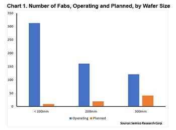
Chart 1. Number of Fabs, Operating and Planned, by Wafer Size
Chart 1, was developed from data in the fab database study. It shows the number of fabs operating and planned by wafer size.
Surprisingly, there are still more than 350 fabs operating at 150mm or smaller. Many manufacture trailing edge devices, especially discretes, while others manufacture relatively new devices, including analog, power, MEMS and LED devices. These semiconductors are not leading-edge devices, but they are essential to many electronics industry end-use products. The die size for many is quite small, and they do not scale well to smaller geometries. Many may continue to be manufactured in 150mm fabs for the immediate future. Others will undoubtedly migrate to 200mm fabs.
There were more than 150 fabs manufacturing devices on 200mm wafers in 2016. Many are producing MOS Logic semiconductors, but there is a sprinkling of 200mm fabs producing a wide variety of other semiconductor product types including analog semiconductors, MEMS devices, power semiconductors, and SRAM. Nineteen new 200mm fabs are planned or under construction.
There were more than 100 fabs operating at 300mm in 2016. These fabs are focused on high-volume devices manufactured at leading-edge technology nodes, including MPUs, DRAM, and NAND Flash. Following the usual pattern, many semiconductor product types will migrate from 200mm to 300mm fabs. More than 40 additional 300mm fabs are planned or under construction.
Chart 2. Wafer Demand by Technology Node
Chart 2, below, developed from data in the wafer demand study, shows wafer demand by technology node.
The first category, greater than or equal to 800nm, was chosen because it represents most manufacturing in 150mm or smaller fabs. The second category, 500nm through 130nm, was chosen because it represents most manufacturing in 200mm fabs. The CAGR for 2016 through 2021 for this category is 4.6%. Most 300mm fabs are at technology nodes beyond 100nm, the third category. The CAGR for 2016 through 2021 for this category is 9.8%.
So, where is the semiconductor manufacturing sweet spot? It depends. The sweet spot for new fabs is 300mm, with 200mm fabs close behind. The sweet spot for wafer demand is 300mm wafers.
Share on:


Testimonial
"We’re proud to call I-Connect007 a trusted partner. Their innovative approach and industry insight made our podcast collaboration a success by connecting us with the right audience and delivering real results."
Julia McCaffrey - NCAB GroupSuggested Items
GlobalFoundries Joins World Economic Forum’s Global Lighthouse Network for Manufacturing Excellence
09/17/2025 | GlobalFoundriesGlobalFoundries announced that the World Economic Forum (WEF) has designated its 300mm fab in Singapore as part of the Global Lighthouse Network (GLN) of advanced manufacturers.
STMicroelectronics to Advance Next-generation Chip Manufacturing Technology with New PLP Pilot Line in Tours, France
09/17/2025 | STMicroelectronicsSTMicroelectronics, a global semiconductor leader serving customers across the spectrum of electronics applications, today announced new details regarding the development of the next generations of Panel-Level Packaging (PLP) technology through a pilot line in its Tours site, France, which is expected to be operational in Q3 2026.
Indium President and CEO to Deliver ELCINA CEO Forum Keynote at Productronica India
09/17/2025 | Indium CorporationIndium Corporation President and CEO Ross Berntson will deliver the Electronic Industries Association of India (ELCINA) CEO Forum keynote at Productronica India, to be held September 17-19 in Bengaluru, India.
Technica USA Advocates for PCBAA Membership Among Printed Circuit Assembly Customers
09/16/2025 | Technica USATechnica USA is actively encouraging its printed circuit assembly customers to join the Printed Circuit Board Association of America (PCBAA), a leading industry organization advocating for increased domestic production of printed circuit boards (PCBs) and substrates.
TTCI and The Training Connection Strengthen Electronics Manufacturing with Test Services and Training at PCB West 2025
09/16/2025 | The Test Connection Inc.The Test Connection Inc. (TTCI), a trusted provider of electronic test and manufacturing solutions, and The Training Connection LLC (TTC-LLC) will exhibit at PCB West 2025, taking place Wednesday, October 1, 2025, at the Santa Clara Convention Center in California. Visitors are invited to Booth 113 to explore the companies’ complementary expertise in test engineering services and workforce development for the electronics industry.