


 The Marketing Minute: Cracking the Code of Technical Marketing
 Trouble in Your Tank: Implementing Direct Metallization in Advanced Substrate Packaging


Building 'OLEDS' From the Ground up for Better Electronics
June 7, 2017 | American Chemical SocietyEstimated reading time: 1 minute
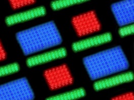
From smartphones to TVs and laptops, light emitting diode (LED) displays are ubiquitous. OLEDs (where the O denotes they are organic, or carbon-based) are among the most energy efficient of these devices, but they generally have higher production costs due to the laborious fabrication processes needed to arrange them properly. Today in ACS Central Science, researchers introduce a new way to efficiently create patterns of OLEDs.
In an LED display, the emissions from red, green and blue diodes are blended to create the white and colored light necessary to render images. It is crucially important to precisely position the different types of diodes in relation to one another. And although many fabrication methods exist, they all have limitations with regard to scalability, pattern control, or feature resolution. Solution-based protocols are attractive because they are inexpensive and well-suited to large scale manufacturing. However, current techniques do not meet the demands required for commercial OLED display technology. Zak Page, Craig Hawker and colleagues at the University of California, Santa Barbara and the Dow Chemical Company sought to overcome this barrier by adopting a bottom-up approach for patterning emissive polymers.
Starting with a substrate of indium tin oxide, the researchers used light-activated chemistry to pinpoint specific locations on the surface for polymer growth. Key to the success of this approach are designer iridium photocatalysts that serve two roles: First, as the catalyst to build the emissive brush polymers, and then as a necessary dopant for the resulting OLED arrays. The authors demonstrated the feasibility of their system by fabricating functional multi-colored OLED arrays and note that their method may enable high throughput manufacturing of OLEDs using many technologies, including inkjet printing, in the future.
Share on:


Testimonial
"We’re proud to call I-Connect007 a trusted partner. Their innovative approach and industry insight made our podcast collaboration a success by connecting us with the right audience and delivering real results."
Julia McCaffrey - NCAB GroupSuggested Items
GlobalFoundries Joins World Economic Forum’s Global Lighthouse Network for Manufacturing Excellence
09/17/2025 | GlobalFoundriesGlobalFoundries announced that the World Economic Forum (WEF) has designated its 300mm fab in Singapore as part of the Global Lighthouse Network (GLN) of advanced manufacturers.
STMicroelectronics to Advance Next-generation Chip Manufacturing Technology with New PLP Pilot Line in Tours, France
09/17/2025 | STMicroelectronicsSTMicroelectronics, a global semiconductor leader serving customers across the spectrum of electronics applications, today announced new details regarding the development of the next generations of Panel-Level Packaging (PLP) technology through a pilot line in its Tours site, France, which is expected to be operational in Q3 2026.
Indium President and CEO to Deliver ELCINA CEO Forum Keynote at Productronica India
09/17/2025 | Indium CorporationIndium Corporation President and CEO Ross Berntson will deliver the Electronic Industries Association of India (ELCINA) CEO Forum keynote at Productronica India, to be held September 17-19 in Bengaluru, India.
Technica USA Advocates for PCBAA Membership Among Printed Circuit Assembly Customers
09/16/2025 | Technica USATechnica USA is actively encouraging its printed circuit assembly customers to join the Printed Circuit Board Association of America (PCBAA), a leading industry organization advocating for increased domestic production of printed circuit boards (PCBs) and substrates.
TTCI and The Training Connection Strengthen Electronics Manufacturing with Test Services and Training at PCB West 2025
09/16/2025 | The Test Connection Inc.The Test Connection Inc. (TTCI), a trusted provider of electronic test and manufacturing solutions, and The Training Connection LLC (TTC-LLC) will exhibit at PCB West 2025, taking place Wednesday, October 1, 2025, at the Santa Clara Convention Center in California. Visitors are invited to Booth 113 to explore the companies’ complementary expertise in test engineering services and workforce development for the electronics industry.