


 The Chemical Connection: The Consequences of Additive Metallizing on Etching Steps
 It’s Only Common Sense: Are You Really So Busy?


UPV/EHU researchers have explored superelasticity properties on a nanometric scale based on shearing an alloy's pillars down to nanometric size. In the article published by the prestigious scientific journal Nature Nanotechnology, the researchers have found that below one micron in diameter the material behaves differently and requires much higher stress for it to be deformed. This superelastic behaviour is opening up new channels in the application of microsystems involving flexible electronics and microsystems that can be implanted into the human body.
Iñaki López-Ferreño, Jose M. San Juan, Maria L. Nó and Jose F. Gómez-Cortés. Photo: UPV/EHU
Superelasticity is a physical property by which it is possible to deform a material to a considerable extent, up to 10%, which is much higher than that of elasticity. So when stress is applied to a straight rod, the rod can form a U-shape and when the stress applied is removed, the rod fully regains its original shape. Although this has been amply proven in macroscopic materials, "until now no one had been able to explore these superelasticity properties in micrometric and nanometric sizes," explained José María San Juan, lead researcher of the article published by Nature Nanotechnology and a UPV/EHU professor.
Researchers in the UPV/EHU's Department of Condensed Matter Physics and Applied Physics II have managed to see that "the superelastic effect is maintained in really small devices in a copper-aluminium-nickel alloy". It is an alloy with shape memory on which the research team has been working for over 20 years on a macroscopic level: Cu-14Al-4Ni, an alloy that displays superelasticity in ambient temperature.
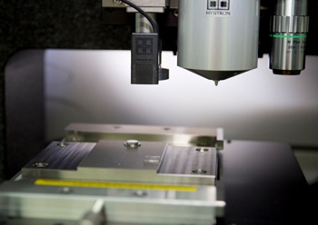
By using a piece of equipment known as a Focused Ion Beam, "an ion cannon that acts as a kind of atomic knife that shears the material", explained San Juan, they built micropillars and nanopillars of this alloy with diameters ranging between 2 µm and 260 nm —a micrometre is one millionth of a metre and a nanometre one thousand-millionth of a metre—. And to them they applied a stress using a sophisticated instrument known as a nanoindenter, which "allows extremely small forces to be applied," and then they measured their behaviour.
The researchers have for the first time confirmed and quantified that in diameters of less than a micrometre there is a considerable change in the properties relating to the critical stress for superelasticity. "The material starts to behave differently and needs a much higher stress for this to take place. The alloy continues to display superelasticity but for much higher stresses". San Juan highlights the novelty of this increase in critical stress linked to size, and also stresses that they have been able to explain the reason for this change in behaviour: "We have proposed an atomic model that allows one to understand why and how the atomic structure of these pillars changes when a stress is applied".
Microsystems involving flexible electronics and devices that can be implanted in the human body
The UPV/EHU professor highlighted the importance of this discovery, "spectacular superelastic behaviour on a small scale", which opens up new channels in the design of strategies for applying alloys with shape memory to develop flexible microsystems and electromechanical nanosystems. "Flexible electronics is very much present on today's market, it is being increasingly used in garments, sports footwear, in various displays, etc." He also affirmed that all this is of crucial importance in developing smart healthcare devices of the Lab-on-a-chip type that can be implanted into the human body. "It will be possible to build tiny micropumps or microactuators that can be implanted on a chip, and which will allow a substance to be released and regulated inside the human body for a range of medical treatments."
It is a discovery that "is expected to have great scientific and technological repercussions and offer the potential to revolutionise various aspects in related fields," concluded San Juan, and he welcomed the fact that "we have managed to transfer all the necessary knowledge and to acquire the working tools that the most advanced centres can avail themselves of to open up a new line of research which can be fully developed at the UPV/EHU".


