


 The Marketing Minute: Cracking the Code of Technical Marketing
 Trouble in Your Tank: Implementing Direct Metallization in Advanced Substrate Packaging


Researchers Image Quasiparticles That Could Lead to Faster Circuits, Higher Bandwidths
June 12, 2017 | Iowa State UniversityEstimated reading time: 2 minutes
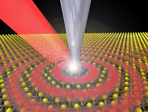
Zhe Fei pointed to the bright and dark vertical lines running across his computer screen. This nano-image, he explained, shows the waves associated with a half-light, half-matter quasiparticle moving inside a semiconductor.
“These are waves just like water waves,” said Fei, an Iowa State University assistant professor of physics and astronomy and an associate of the U.S. Department of Energy’s Ames Laboratory. “It’s like dropping a rock on the surface of water and seeing waves. But these waves are exciton-polaritons.”
Exciton-polaritons are a combination of light and matter. Like all quasiparticles, they’re created within a solid and have physical properties such as energy and momentum. In this study, they were launched by shining a laser on the sharp tip of a nano-imaging system aimed at a thin flake of molybdenum diselenide (MoSe2), a layered semiconductor that supports excitons.
Excitons can form when light is absorbed by a semiconductor. When excitons couple strongly with photons, they create exciton-polaritons.
It’s the first time researchers have made real-space images of exciton-polaritons. Fei said past research projects have used spectroscopic studies to record exciton-polaritons as resonance peaks or dips in optical spectra. Until recent years, most studies have only observed the quasiparticles at extremely cold temperatures – down to about -450 degrees Fahrenheit.
But Fei and his research group worked at room temperature with the scanning near-field optical microscope in his campus lab to take nano-optical images of the quasiparticles.
“We are the first to show a picture of these quasiparticles and how they propagate, interfere and emit,” Fei said.
The researchers, for example, measured a propagation length of more than 12 microns – 12 millionths of a meter – for the exciton-polaritons at room temperature.
Fei said the creation of exciton-polaritons at room temperature and their propagation characteristics are significant for developing future applications for the quasiparticles. One day they could even be used to build nanophotonic circuits to replace electronic circuits for nanoscale energy or information transfer.
Fei said nanophotonic circuits with their large bandwidth could be up to 1 million times faster than current electrical circuits.
A research team led by Fei recently reported its findings in the scientific journal Nature Photonics. The paper’s first author is Fengrui Hu, an Iowa State postdoctoral research associate in physics and astronomy. Additional co-authors are Yilong Luan, an Iowa State doctoral student in physics and astronomy; Marie Scott, a recently graduated undergraduate at the University of Washington; Jiaqiang Yan and David Mandrus of Oak Ridge National Laboratory and the University of Tennessee; and Xiaodong Xu of the University of Washington.
The researchers’ work was supported by funds from Iowa State and the Ames Laboratory to launch Fei’s research program. The W.M. Keck Foundation of Los Angeles also partially supported the nano-optical imaging for the project.
The researchers also learned that by changing the thickness of the MoSe2 semiconductor, they could manipulate the properties of the exciton-polaritons.
Fei, who has been studying quasiparticles in graphene and other 2-D materials since his graduate school days at University of California San Diego, said his earlier work opened the doors for studies of exciton-polaritons.
“We need to explore further the physics of exciton-polaritons and how these quasiparticles can be manipulated,” he said.
That could lead to new devices such as polariton transistors, Fei said. And that could one day lead to breakthroughs in photonic and quantum technologies.
Share on:


Testimonial
"The I-Connect007 team is outstanding—kind, responsive, and a true marketing partner. Their design team created fresh, eye-catching ads, and their editorial support polished our content to let our brand shine. Thank you all! "
Sweeney Ng - CEE PCBSuggested Items
MEMS & Imaging Sensors Summit to Spotlight Sensing Revolution for Europe’s Leadership
09/11/2025 | SEMIIndustry experts will gather November 19-20 at the SEMI MEMS & Imaging Sensors Summit 2025 to explore the latest breakthroughs in AI-driven MEMS and imaging optimization, AR/VR technologies, and advanced sensor solutions for critical defence applications.
Direct Imaging System Market Size to Hit $4.30B by 2032, Driven by Increasing Demand for High-Precision PCB Manufacturing
09/11/2025 | Globe NewswireAccording to the SNS Insider, “The Direct Imaging System Market size was valued at $2.21 Billion in 2024 and is projected to reach $4.30 Billion by 2032, growing at a CAGR of 8.68% during 2025-2032.”
I-Connect007’s Editor’s Choice: Five Must-Reads for the Week
07/04/2025 | Marcy LaRont, I-Connect007For our industry, we have seen several bullish market announcements over the past few weeks, including one this week by IDC on the massive growth in the global server market. We’re also closely watching global trade and nearshoring. One good example of successful nearshoring is Rehm Thermal Systems, which celebrates its 10th anniversary in Mexico and the official opening of its new building in Guadalajara.
Driving Innovation: Direct Imaging vs. Conventional Exposure
07/01/2025 | Simon Khesin -- Column: Driving InnovationMy first camera used Kodak film. I even experimented with developing photos in the bathroom, though I usually dropped the film off at a Kodak center and received the prints two weeks later, only to discover that some images were out of focus or poorly framed. Today, every smartphone contains a high-quality camera capable of producing stunning images instantly.
United Electronics Corporation Advances Manufacturing Capabilities with Schmoll MDI-ST Imaging Equipment
06/24/2025 | United Electronics CorporationUnited Electronics Corporation has successfully installed the advanced Schmoll MDI-ST (XL) imaging equipment at their advanced printed circuit board facility. This significant technology investment represents a continued commitment to delivering superior products and maintaining their position as an industry leader in precision PCB manufacturing.