


 The Marketing Minute: Cracking the Code of Technical Marketing
 Trouble in Your Tank: Implementing Direct Metallization in Advanced Substrate Packaging


Batteries from Scrap Metal
June 14, 2017 | WileyEstimated reading time: 2 minutes
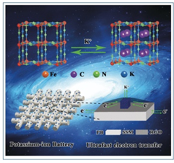
Chinese scientists have made good use of waste while finding an innovative solution to a technical problem by transforming rusty stainless steel mesh into electrodes with outstanding electrochemical properties that make them ideal for potassium-ion batteries. As reported in the journal Angewandte Chemie, the rust is converted directly into a compact layer with a grid structure that can store potassium ions. A coating of reduced graphite oxide increases the conductivity and stability during charge/discharge cycles.
Increasing use of renewable energy requires effective energy storage within the grid. Lithium ion batteries, widely used in portable electronics, are promising candidates. Lithium ion batteries are based on the displacement of lithium ions. While charging, the ions move toward the graphite electrode, where they are stored between the layers of carbon. When discharging, they are released. However, lithium is expensive and reserves are limited. Sodium ion batteries have been explored as an alternative.
“Potassium ions are just as inexpensive and readily available as sodium, and potassium ion batteries would be superior from the electric aspect,” reports Xin-Bo Zhang. “However, the significantly larger radius of the potassium ions has posed a problem. Repeated storage and release of these ions destabilizes the materials currently used in electrodes.”
Zhang and a team from the Chinese Academy of sciences and Jilin University (Changchun, China) have now found an elegant solution in their use of a waste material to make novel electrodes: rejected stainless steel mesh from filters and sieves. Despite the excellent durability of these grids, harsh conditions do lead to some corrosion. The metal can be reclaimed in a furnace, but this process requires a great deal of money, time, and energy, as well as producing emissions. Says Zhang: “Conversion into electrodes could develop into a more ecologically and economically sensible form of recycling.”
The corroded mesh is dipped into a solution of potassium ferrocyanide (yellow prussiate of potash, known as a fining agent for wine). This dissolves iron, chromium, and nickel ions out of the rust layer. These combine with ferricyanide ions into the complex salt known as Prussian blue, a dark blue pigment that is deposited onto the surface of the mesh as scaffold-like nanocubes. Potassium ions can easily and rapidly be stored in and released from these structures.
The researchers then use a dip-coating process to deposit a layer of graphene oxide (oxidized graphite layers). This layer nestles tightly onto the nanocubes. Subsequent reduction converts the graphene oxide to reduced graphene oxide (RGO), which consists of layers of graphite with isolated oxygen atoms. Zhang explains, “the RGO coating inhibits clumping and detachment of the active material. At the same time, it significantly increases the conductivity and opens ultrafast electron-transport pathways.”
In tests, coin cells made with these new electrodes demonstrate excellent capacity, discharge voltages, rate capability, and outstanding cycle stability. Because the inexpensive, binder-free electrodes are very flexible, they are highly suitable for use in flexible electronic devices.
Share on:


Testimonial
"The I-Connect007 team is outstanding—kind, responsive, and a true marketing partner. Their design team created fresh, eye-catching ads, and their editorial support polished our content to let our brand shine. Thank you all! "
Sweeney Ng - CEE PCBSuggested Items
Beyond Design: Slaying Signal Integrity Villains
09/17/2025 | Barry Olney -- Column: Beyond DesignHigh-speed PCB design is a balancing act, where subtle oversights can develop into major signal integrity nightmares. Some culprits lie dormant during early validation, only to reveal themselves later through workflow disruptions and elusive performance bottlenecks. Take crosstalk, for example. What begins as a stray signal coupling between traces can ripple through the design, ultimately destabilizing the power distribution network. Each of these troublemakers operates with signature tactics, but they also have well-known vulnerabilities.
Driving Innovation: Depth Routing Processes—Achieving Unparalleled Precision in Complex PCBs
09/08/2025 | Kurt Palmer -- Column: Driving InnovationIn PCB manufacturing, the demand for increasingly complex and miniaturized designs continually pushes the boundaries of traditional fabrication methods, including depth routing. Success in these applications demands not only on robust machinery but also sophisticated control functions. PCB manufacturers rely on advanced machine features and process methodologies to meet their precise depth routing goals. Here, I’ll explore some crucial functions that empower manufacturers to master complex depth routing challenges.
Global PCB Connections: Understanding the General Fabrication Process—A Designer’s Hidden Advantage
08/14/2025 | Markus Voeltz -- Column: Global PCB ConnectionsDesigners don’t need to become fabricators, but understanding the basics of PCB fabrication can save you time, money, and frustration. The more you understand what’s happening on the shop floor, the better you’ll be able to prevent downstream issues. As you move into more advanced designs like HDI, flex circuits, stacked vias, and embedded components, this foundational knowledge becomes even more critical. Remember: the fabricator is your partner.
I-Connect007 Editor’s Choice: Five Must-Reads for the Week
08/08/2025 | Andy Shaughnessy, I-Connect007If you’ve been watching the news lately, you might be tempted to opine, “What’s going on here?” In this week’s must-reads, we have a wrap-up of the latest news about U.S. tariffs with Asia, and columnist Tom Yang explains why some PCB fabrication business should remain in China. We also have a piece that examines the unprecedented growth that green manufacturing is expected to see over the next four years.
Driving Innovation: Inner Layer Alignment Methods in PCB Production
08/06/2025 | Kurt Palmer -- Column: Driving InnovationIn PCB manufacturing, precision is a fundamental requirement. Among many complex processes, the accurate registration of inner layers before lamination is one of the most critical. Much like a child's game where rings must be perfectly stacked onto a single pin, PCB manufacturers align multiple conductive and insulating layers to form a cohesive, functional board. This alignment directly affects PCB precision; tighter layer alignment results in smaller "annular rings," superior performance, and higher yields.