


 Global Citizenship: Together for a Perfect PCB Solution
 Smart Automation: Odd-form Assembly—Dedicated Insertion Equipment Matters
 Nolan’s Notes: Everyone Has Their Eye on India


AOI Capabilities Study with 03015 Components
June 14, 2017 | David Geiger, et al., Flex InternationalEstimated reading time: 4 minutes
Abstract
Automated optical inspection (AOI) is advantageous in that it enables defects to be detected early in the manufacturing process, reducing the cost of repair as the AOI systems identify the specific components that are failing removing the need for any additional test troubleshooting. Because of this, more electronic contract manufacturing services (EMS) companies are implementing AOI into their SMT lines to minimize repair costs and maintain good process and product quality, especially for new component types. This project focuses on the testing of component package 03015 which is challenging for AOI.
Highly-automated and effective test methods are becoming a more and more important topic in our industry today. Advances in modern manufacturing technologies have been making factories smarter, safer, and also more environmentally sustainable. Finding and implementing smart machines which provide real time information is critical to success. Currently, we have been successful in using 2D/3D AOI for production; however not for the upcoming 03015 components. Therefore, we are working with AOI vendors to ensure successful testing of this component type, with a special emphasis on optimizing algorithm threshold settings to detect defects.
We have been working with five AOI vendors with five test vehicles (PCBAs). Each PCBA board has 246 components with three different pitch sizes (100 µm, 150 µm, 200 µm). The results of Attribute GR&R, Defect Escapes, and False Call PPM (parts per million) will be presented.
Based on the data which we received up to now, every set of data (five sets—still waiting for results of AOI System 3) is from the algorithms of 2D AOI, although some machines have the 3D AOI capability. These machines have shown different levels of performance. AOI System 5’s results have an excellent acceptable level for Attribute GR&R; both AOI System 5 and AOI System 6 have only several percentage points of a Defect Escape rate. However, this study is just in its infancy; more improvement and testing will be performed. We will continue to provide new test results from all suppliers.
Introduction
The printed circuit board assembly (PCBA) industry has long embraced the smaller, lighter, faster mantra for electronic devices, especially in recent years. With the increasing use of smaller components, more consideration is required to study and implement changes; not only for SMT processes, but also for testing. There have been some studies conducted for SPI (solder paste inspection) with 03015 components, however, there are very few recommended practices for AOI.
The 03015 [0.3 mm x 0.15 mm] device is a microchip component. For reference, please note that a human hair is approximately 0.1mm. To ensure a successful implementation of the 03015 components, besides for these three critical areas—placement equipment, assembly materials, and process control—the capabilities of machines used to test these component types is another critical consideration. Now, 3D SPI is more commonly used in the SMT process, and 3D AOI is quickly catching up.
During the initial stage of our study, we first tested these five boards with 03015 components on our 2D AOI machine in our Milpitas manufacturing site. Next, we provided the boards to the R&D labs of five AOI vendors who all have 3D AOI machines. Working with various R&D engineers, it was obvious this was a challenging task for their current AOI systems, especially for 3D AOI systems due to component reflection.
Our test data and results showed that the 2D AOI machines have different capabilities in detecting defects for 03015, such as misalignment, tombstoning, and shorts. While the defect escape percentage decreased, false call PPM increased, therefore, optimized programming should be based on test data analysis.
Experiments
In total, we asked five AOI vendors (R&D engineers) to work on this project. We received four sets of test data—AOI System 3 data is to be provided later. The test procedure is the same for all machines with five boards.
Test Vehicle
Figure 1: Company Miniaturized Test Vehicle
Five boards with 03015 components were tested on the AOI machines. Figure 1 is our test vehicle, which has three areas for different pitch sizes. The pitch areas are indicated as different color arrows: red color (A – 100 µm), yellow color (B – 150 µm), and blue color (C – 200 µm).
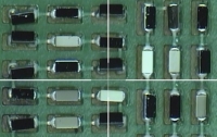
The 03015 component was a production resistor: 292 µm, 143 µm, and 100 µm corresponding to its length, width, and height, respectively, as shown in Figure 2, where area A is without fab mask. There are a total of 87, 81, and 78 components in areas A, B, and C, respectively. The pad size (length, width) is 150 µm by 150 µm on the PCB fab. Figure 3 shows pictures for area A (right column), area B (center column), and area C (left column); after print (top row), after placement (center row), and after reflow (bottom row). There are different colors for optical pictures due to 03015 component reflection, which increased AOI testing difficulty.
Figure 2: Three areas of 03015 components.
Figure 3: Optical picture: after print (top), after placement (center), and after reflow (bottom).
To read the full version of this article, which appeared in the June 2017 issue of SMT Magazine, click here.
Share on:


Testimonial
"Our marketing partnership with I-Connect007 is already delivering. Just a day after our press release went live, we received a direct inquiry about our updated products!"
Rachael Temple - AlltematedSuggested Items
Koh Young, Fuji, and Kurtz ERSA Drive Smart Manufacturing Solutions for EV and Automotive Electronics at Kunshan, China Technical Seminar
09/11/2025 | Koh YoungKoh Young Technology, the global leader in True 3D measurement-based inspection solutions, partnered with Fuji Corporation and Kurtz ERSA to host an exclusive technical seminar for leading automotive manufacturers in East China. Held on September 4 at Fuji’s factory in Kunshan, the event gathered participants representing over 35 companies.
MacDermid Alpha Presents at SMTA New Delhi, Bangalore Chapter, on Flux–OSP Interaction
09/09/2025 | MacDermid Alpha Electronics SolutionsMacDermid Alpha contributes technical insights on OSP solderability at the Bangalore Chapter, SMTA reinforcing commitment to knowledge-sharing and industry collaboration.
Electra’s ElectraJet EMJ110 Inkjet Soldermask Now in Black & Blue at Sunrise Electronics
09/08/2025 | Electra Polymers LtdFollowing the successful deployment of Electra’s Green EMJ110 Inkjet Soldermask on KLA’s Orbotech Neos™ platform at Sunrise Electronics in Elk Grove Village, Illinois, production has now moved beyond green.
Absolute EMS: The Science of the Perfect Solder Joint
09/05/2025 | Absolute EMS, Inc.Absolute EMS, Inc., a six-time award-winning provider of fast turnaround, turnkey contract electronic manufacturing services (EMS), is drawing attention to the critical role of 3D Solder Paste Inspection (SPI) in ensuring the reliability of both FLEX and rigid printed circuit board assemblies (PCBAs).
Indium Corporation to Highlight High-Reliability Solder Solutions at SMTA Guadalajara Expo
09/04/2025 | Indium CorporationIndium Corporation, a leading materials refiner, smelter, manufacturer, and supplier to the global electronics, semiconductor, thin-film, and thermal management markets, will feature a range of innovative, high-reliability solder products for printed circuit board assembly (PCBA) at the SMTA Guadalajara Expo and Tech Forum, to be held September 17-18 in Guadalajara, Mexico.