


 The Marketing Minute: Cracking the Code of Technical Marketing
 Trouble in Your Tank: Implementing Direct Metallization in Advanced Substrate Packaging


New Prospects for Universal Memory
June 21, 2017 | MIPTEstimated reading time: 4 minutes
Researchers from MIPT’s Center of Shared Research Facilities have found a way to control oxygen concentration in tantalum oxide films produced by atomic layer deposition. These thin films could be the basis for creating new forms of nonvolatile memory. The paper was published in the journal ACS Applied Materials & Interfaces, which has an impact factor of 7.14.
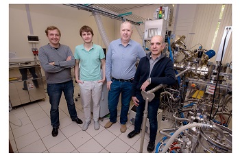
(From left) Dmitry Kuzmichev, Konstantin Egorov, Andrey Markeev, and Yury Lebedinskiy posing next to the atomic layer deposition apparatus at the Center of Shared Research Facilities, MIPT
Want nonvolatile memory that’s fast as RAM and has the capacity of flash?
Because data storage and processing solutions are so central to modern technology, many research teams and companies are pursuing new types of computer memory. One of their major goals is to develop universal memory — a storage medium that would combine the high speed of RAM with nonvolatility of a flash drive.
A promising technology for creating such a device is resistive switching memory, or ReRAM. It works by changing the resistance across a memory cell as a result of applied voltage. Since each cell has a high- and a low-resistance state, it can be used to store information, e.g., in the form of zeros and ones.
A ReRAM cell can be realized as a metal-dielectric-metal structure. Oxides of transition metals such as hafnium and tantalum have proved useful as the dielectric component of this layered structure. Applying voltage to a memory cell that is based on these materials causes oxygen migration, changing its resistance. This makes the distribution of oxygen concentration in the oxide film a crucial parameter determining the functional properties of the memory cell.
However, despite significant advances in ReRAM development, flash memory shows no sign of losing ground. The reason for this is that flash memory allows for three-dimensional memory cell stacking, which enables a much greater storage density. In contrast to this, oxygen-deficient film deposition techniques normally used in ReRAM design are not applicable to functional 3-D architectures.
That’s where atomic layer deposition comes in
In a bid to find an alternative technique, MIPT researchers turned to atomic layer deposition, a chemical process by which thin films can be produced on the surface of a material. During the last decade, ALD has become increasingly widespread, with numerous applications in nanoelectronics, optics, and the biomedical industry. There are two major advantages to atomic layer deposition. The first one is the unprecedented control over film thickness: It is possible to deposit films that are several nanometers thick with an error of a fraction of a nanometer. The other advantage is that ALD enables conformal coating of 3-D structures, which is problematic for most of the currently used nanofilm deposition techniques.
In an ALD process, a substrate is sequentially exposed to two chemicals that are known as the precursor and the reactant. It is the chemical reaction between these two substances that produces a coating layer. In addition to the element used in the coating, precursors contain other compounds — e.g., of carbon or chlorine — called ligands. They facilitate the reaction but, in an ideal ALD process, have to be completely removed from the resulting film once the interaction with the other chemical (reactant) has occurred. It is vital to choose the right substances for use in atomic layer deposition. Although it proves difficult to deposit oxide films with variable oxygen concentration by ALD, they are essential for ReRAM.
“The hardest part in depositing oxygen-deficient films was finding the right reactants that would make it possible to both eliminate the ligands contained in the metallic precursor and control oxygen content in the resulting coating,” says Andrey Markeev, who holds a PhD in physics and mathematics and is a leading researcher at MIPT. “We achieved this by using a tantalum precursor, which by itself contains oxygen, and a reactant in the form of plasma-activated hydrogen.”
Stages of chemical reactions involved in the deposition of oxygen-deficient tantalum oxide films (left) and the results of their analysis by X-ray photoelectron spectroscopy (right)
Experimental cluster for growing and studying thin films in a vacuum at the Center of Shared Research Facilities, MIPT
Confirming the experimental findings turned out to be a challenge in itself. As soon as the experimental sample is removed from the vacuum chamber, which houses it during ALD, and exposed to the atmosphere, this causes modifications in the top layer of the dielectric, making it impossible to detect oxygen deficiency using analytic techniques such as electron spectroscopy, which target the surface of the sample.
“In this study, we needed not just to obtain the films containing different amounts of oxygen but also to confirm this experimentally,” says Konstantin Egorov, a PhD student at MIPT. “To do this, our team worked with a unique experimental cluster, which allowed us to grow films and study them without breaking the vacuum.”
The study was supported by the Russian Science Foundation Grant No. 14-19-01645 and MIPT’s 5-100 Program under the Russian Academic Excellence Project. The researchers made use of the sophisticated scientific equipment for research in the field of nanotechnology, provided by MIPT’s Center of Shared Research Facilities.
Share on:


Testimonial
"In a year when every marketing dollar mattered, I chose to keep I-Connect007 in our 2025 plan. Their commitment to high-quality, insightful content aligns with Koh Young’s values and helps readers navigate a changing industry. "
Brent Fischthal - Koh YoungSuggested Items
PC Graphics Add-in Board Shipments Up 27% QoQ in 2Q25
09/03/2025 | Jon Peddie ResearchAccording to a new research report from the analyst firm Jon Peddie Research, the growth of the global PC-based graphics add-in board market reached 11.6 million units in Q2'25 and desktop PC CPUs shipments increased to 21.7 million units.
PC GPU Shipments Up 8.4% in 2Q25 on Pre-Tariff Demand
09/02/2025 | Jon Peddie ResearchJon Peddie Research reports the growth of the global PC-based graphics processor unit (GPU) market reached 74.7 million units in Q2'25, and PC CPU shipments increased to 66.9 million units.
20 Years of Center Nanoelectronic Technologies (CNT) – Backbone of German Semiconductor Research Celebrates Anniversary
08/14/2025 | Fraunhofer IPMSThe Center Nanoelectronic Technologies (CNT) of the Fraunhofer Institute for Photonic Microsystems (IPMS) is celebrating its 20th anniversary this year. Since its founding in 2005, it has developed into a pillar of applied semiconductor research in Germany and Europe. With its unique research cleanroom and equipment adhering to the 300-mm wafer industry standard, CNT is unparalleled in Germany and serves as a central innovation driver for the microelectronics industry.
Q2 Client CPU Shipments Increased 8% from Last Quarter, Up 13% YoY
08/13/2025 | Jon Peddie ResearchJon Peddie Research reports that the global client CPU market expanded for two quarters in a row, and in Q2’25, it showed unseasonal growth of 7.9% from last quarter, while server CPU shipments increased 22% year over year.
FuriosaAI Closes $125M Investment Round to Scale Production of Next-Gen AI Inference Chip
07/31/2025 | BUSINESS WIREFuriosaAI, a semiconductor company building a new foundation for AI compute, today announced it has completed a $125 million Series C bridge funding round. The investment continues a period of significant momentum for Furiosa as global demand for high-performance, efficient AI infrastructure soars.