


 The Marketing Minute: Cracking the Code of Technical Marketing
 Trouble in Your Tank: Implementing Direct Metallization in Advanced Substrate Packaging


Perovskite Photovoltaics Market, 2028
June 30, 2017 | PRNewswireEstimated reading time: 2 minutes
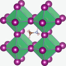
Research and Markets has announced the addition of the "Perovskite Photovoltaics 2018-2028" report to their offering.
As one of the top ten science breakthroughs of 2013, perovskite solar cells have shown potential both in the rapid efficiency improvement (from 2.2% in 2006 to the latest record 20.1% in 2014) and in cheap material and manufacturing costs. Perovskite solar cells have attracted tremendous attention from the likes of DSSC and OPVs with greater potential. Many companies and research institutes that focused on DSSCs and OPVs now transfer attention to perovskites with few research institutes remaining exclusively committed to OPVs and DSSCs.
Perovskite solar cells are a breath of fresh air into the emerging photovoltaic technology landscape. They have amazed with an incredibly fast efficiency improvement, going from just 2% in 2006 to over 20.1% in 2015.
Photovoltaic (PV) technologies are basically divided into two big categories: wafer-based PV (also called 1st generation PV) and thin-film cell PV.
Traditional crystalline silicon (c-Si) cells (both single crystalline silicon and multi-crystalline silicon) and gallium arsenide (GaAs) cells belong to the wafer-based PVs. Among different single-junction solar technologies, GaAs exhibits the highest efficiency, followed by c-Si cells. The latter dominates the current PV market (about 90% market share).
Thin-film cells normally absorb light 10-100 times more efficiently than silicon, allowing the use of films of just a few microns thick. Cadmium telluride (CdTe) technology has been successfully commercialized, with more than 20% cell efficiency and 17.5% module efficiency record. CdTe cells currently take about 5% of the total market. Other commercial thin-film technologies include hydrogenated amorphous silicon (a-Si:H) and copper indium gallium (di)selenide (CIGS) cells, taking approximately 2% market share each today. Copper zinc tin sulphide technology has been developed for years and it will still require some time for real commercialization.
The emerging thin-film PVs are also called 3rd generation PVs, which refer to PVs using technologies that have the potential to overcome Shockley-Queisser limit or are based on novel semiconductors. The 3rd generation PVs include DSSC, organic photovoltaic (OPV), quantum dot (QD) PV and perovskite PV. The cell efficiencies of perovskite are approaching that of commercialized 2nd generation technologies such as CdTe and CIGS. Other emerging PV technologies are still struggling with lab cell efficiencies lower than 15%.
High and rapidly improved efficiencies, as well as low potential material & processing costs are not the only advantages of perovskite solar cells. Flexibility, semi-transparency, tailored form factors, thin-film, light-weight are other value propositions of perovskite solar cells.
With so many improvements, perovskite solar cell technology is still in the early stages of commercialization compared with other mature solar technologies as there are a number of concerns remaining such as stability, toxicity of lead in the most popular perovskite materials, scaling-up, etc. Crystalline silicon PV modules have fallen from $76.67/W in 1977 to $0.4-0.5/W with fair efficiency in early 2015.
Share on:


Testimonial
"Advertising in PCB007 Magazine has been a great way to showcase our bare board testers to the right audience. The I-Connect007 team makes the process smooth and professional. We’re proud to be featured in such a trusted publication."
Klaus Koziol - atgSuggested Items
Trouble in Your Tank: Implementing Direct Metallization in Advanced Substrate Packaging
09/15/2025 | Michael Carano -- Column: Trouble in Your TankDirect metallization systems based on conductive graphite are gaining popularity throughout the world. The environmental and productivity gains achievable with this process are outstanding. Direct metallization reduces the costs of compliance, waste treatment, and legal issues related to chemical exposure. A graphite-based direct plate system has been devised to address these needs.
Closing the Loop on PCB Etching Waste
09/09/2025 | Shawn Stone, IECAs the PCB industry continues its push toward greener, more cost-efficient operations, Sigma Engineering’s Mecer System offers a comprehensive solution to two of the industry’s most persistent pain points: etchant consumption and rinse water waste. Designed as a modular, fully automated platform, the Mecer System regenerates spent copper etchants—both alkaline and acidic—and simultaneously recycles rinse water, transforming a traditionally linear chemical process into a closed-loop system.
Driving Innovation: Depth Routing Processes—Achieving Unparalleled Precision in Complex PCBs
09/08/2025 | Kurt Palmer -- Column: Driving InnovationIn PCB manufacturing, the demand for increasingly complex and miniaturized designs continually pushes the boundaries of traditional fabrication methods, including depth routing. Success in these applications demands not only on robust machinery but also sophisticated control functions. PCB manufacturers rely on advanced machine features and process methodologies to meet their precise depth routing goals. Here, I’ll explore some crucial functions that empower manufacturers to master complex depth routing challenges.
Trouble in Your Tank: Minimizing Small-via Defects for High-reliability PCBs
08/27/2025 | Michael Carano -- Column: Trouble in Your TankTo quote the comedian Stephen Wright, “If at first you don’t succeed, then skydiving is not for you.” That can be the battle cry when you find that only small-diameter vias are exhibiting voids. Why are small holes more prone to voids than larger vias when processed through electroless copper? There are several reasons.
The Government Circuit: Navigating New Trade Headwinds and New Partnerships
08/25/2025 | Chris Mitchell -- Column: The Government CircuitAs global trade winds continue to howl, the electronics manufacturing industry finds itself at a critical juncture. After months of warnings, the U.S. Government has implemented a broad array of tariff increases, with fresh duties hitting copper-based products, semiconductors, and imports from many nations. On the positive side, tentative trade agreements with Europe, China, Japan, and other nations are providing at least some clarity and counterbalance.