


 It’s Only Common Sense: Create Passion That Customers Feel
 Punching Out: How to Stay Focused in Business and M&A


It is ultra-bright, electrically conductive on the edge and highly insulating inside - and also at room temperature: physicists from the University of Würzburg have developed a new material that promises a lot.
The material class of topological insulators is currently the focus of international solid-state research. These substances are electrically insulative in the interior, because the electrons remain strongly bound to the atoms. On the surface, however, nature has provided them with a conductive shell due to quantum effects.
In addition, the built-in compass needle of the electron, the "spin", whose orientation can very efficiently transmit information, is protected against movement by these surface channels. With these features, topological insulators could make an old dream come true: a spin-based data processing-the so-called spintronics.
Previous concepts only work in the refrigerator
So far, however, there has been a major obstacle to the technical use of such surface channels: "As the temperature of a topological insulator increases, all quantum effects are washed out and the special properties of the electrically conductive edges," explains Privatdozent Dr. Jörg Schäfer from the Chair of Experimental Physics 4, University of Würzburg.
For this reason, all known topological insulators must be cooled to very low temperatures - usually down to minus 270 degrees Celsius - in order to study the quantum properties of the edge channels. "Possible applications, for example for ultra-fast electronics or in a quantum computer, are of course not particularly practical under such conditions," says the physicist.
A team from Würzburg physicists has now presented a completely new concept to deal with this problem elegantly. Involved in this were experimental physicists from the Department of Experimental Physics IV, Professor Ralph Claessen and Professor Dr. Jörg Schäfer, as well as the theorists from the Department of Theoretical Physics I, Professor Ronny Thomale, Professor Werner Hanke and Dr. Gang Li. The scientists have now published the results of their work in the latest issue of Science .
Targeted material design
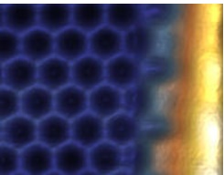
A special material combination is the basis of the Würzburg breakthrough: an ultra-thin layer of a single layer of bismuth atoms, which is applied to a support of silicon carbide.
What makes this combination so special? "The crystalline structure of the silicon carbide carrier results in the deposition of the bismuth film into a honeycomb-like arrangement of the bismuth atoms-similar to the structure of the material of the material, which is composed of carbon atoms," explains Professor Ralph Claessen. Because of this analogy, the ultra-thin film is called "bismuth".
However, there is a crucial difference to the graph: "Bismuth is a chemical bond to the substrate," explains Professor Ronny Thomale. However, this plays a central role in the new concept so that the material has the desired electronic properties. A computer-aided modeling demonstrates this very clearly: "While conventional bismuth is an electrically conductive metal, the honeycomb-like monolayer remains a pronounced insulator, even at room temperature and far above it," says the physicist. It is only through the ingenious combination of the heavy bismuth atoms with the silicon carbide substrate, which is also insulating, that this artificially desired initial situation can be produced artificially.
Electronautobahn in edge position
The electronic conduction paths come into play at the edge of a bismuth piece. There are the metal edge channels, which are to be used in the data processing of the future. Not only did the theoretical considerations of the Würzburg research team reveal this; Using microscopic techniques, the physicists were able to prove the state clearly in the experiment.
However, for the usability of the edge channels in electronic components, it is essential that there is no short circuit through the inside of the topological material or through the substrate. "In previous topological insulators this had to be ensured by means of extreme cooling", explains Jörg Schäfer. With the new Bismuten concept, however, this effort is no longer necessary: due to the pronounced insulator behavior of the layer and the support, no interfering short circuits are possible.
According to the Würzburg scientists, this leap forward to the ability to function at room temperature makes the discovery interesting for potential applications under realistic conditions. "Such management channels are 'topologically protected', that is, they can transmit information almost without loss," explains Ralph Claessen. Since the transmission of data with few electron spins - the Spintronics - is conceivable in this way, the Würzburg team hopes to make great progress towards more efficient information technology.
Result of cooperative research
This breakthrough in the research field of topological physics is a direct result of the close cooperation between the Würzburg physicists within the framework of the DFG-funded special research area SFB1170 "ToCoTronics" (Topological and Correlated Electronics at Surfaces and Interfaces).


