-
- News
- Books
Featured Books
- pcb007 Magazine
Latest Issues
Current IssueSales: From Pitch to PO
From the first cold call to finally receiving that first purchase order, the July PCB007 Magazine breaks down some critical parts of the sales stack. To up your sales game, read on!
The Hole Truth: Via Integrity in an HDI World
From the drilled hole to registration across multiple sequential lamination cycles, to the quality of your copper plating, via reliability in an HDI world is becoming an ever-greater challenge. This month we look at “The Hole Truth,” from creating the “perfect” via to how you can assure via quality and reliability, the first time, every time.
In Pursuit of Perfection: Defect Reduction
For bare PCB board fabrication, defect reduction is a critical aspect of a company's bottom line profitability. In this issue, we examine how imaging, etching, and plating processes can provide information and insight into reducing defects and increasing yields.
- Articles
- Columns
- Links
- Media kit
||| MENU - pcb007 Magazine
Epec Now Offering PCB Layout and Design Services
July 21, 2017 | EpecEstimated reading time: 1 minute

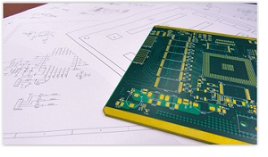
Epec Engineered Technologies, one of America’s oldest printed circuit board (PCB) manufacturers located outside of Boston, Massachusetts, is now offering PCB layout and design services to their customers.
Founded in 1952, Epec has a long history with circuit boards and the PCB industry. Over the past 65 years, Epec has worked on countless circuit board parts for some of the top tier OEMs in the electronics industry. From having PCBs on the Apollo 11 spaceflight, which landed the first humans on the Moon, to their recent advancements in heavy and extreme copper circuit boards, Epec’s sixty-five year history of innovation has truly made them a thought leader amongst the electronics community.
Ed McMahon, CEO of Epec, said, “We have been offering PCB layout and design services a while now, we just never had a large demand for it. In the past when a customer came to us looking for PCB design help, we wouldn’t turn them away; it was just not an advertised offering in our product line.”
Epec’s PCB layout and design services encompass a full design flow including rules driven designs, schematic capture, library development, database construction and verification, signal integrity/design verification, EMI checking and many others.
McMahon added, “We are now seeing more and more companies come to us to help them with their circuit board layout needs. Having the resources in-house allows us to be an extension of our customers engineering teams. We’ve also seen the benefits of customers having their PCB layout and design done by the same company that will be manufacturing their boards as it helps to reduce cost by only designing exactly what they need.”
As Epec continues to expand their PCB supply chain and services, they do so with one goal in mind; to provide their valued customers what they need and when they need it.
About Epec, LLC
Epec Engineered Technologies is the ideal choice for an OEM seeking customized product solutions from a focused and agile partner having supported over 5,000 customers across all sectors of the electronics industry. By providing highly experienced technical resources, a proven manufacturing platform and the fastest delivery in the industry, we are able to provide cost effective and innovative solutions that deliver the highest reliability products to the market faster. Click here for more information.
Testimonial
"In a year when every marketing dollar mattered, I chose to keep I-Connect007 in our 2025 plan. Their commitment to high-quality, insightful content aligns with Koh Young’s values and helps readers navigate a changing industry. "
Brent Fischthal - Koh YoungSuggested Items
MKS Showcases Next-generation PCB Manufacturing Solutions at the Thailand Electronics Circuit Asia 2025
08/06/2025 | MKS Instruments, Inc.MKS Inc, a global provider of enabling technologies that transform our world, today announced its participation in Thailand Electronics Circuit Asia 2025 (THECA 2025), taking place August 20–22 at BITEC in Bangkok.
Point2 Technology, Foxconn Interconnect Technology Partner to Revolutionize AI Cluster Scalability with Terabit-Speed Interconnect
08/06/2025 | BUSINESS WIREPoint2 Technology, a leading provider of ultra-low-power, low-latency mixed-signal SoC solutions for multi-terabit interconnect, and Foxconn Interconnect Technology (FIT), a global leader in precision interconnect solutions, have signed a Memorandum of Understanding (MOU) to accelerate the commercialization of next-generation Active RF Cable (ARC) and Near Pluggable e-Tube (NPE) solutions.
Advancing Electrolytic Copper Plating for AI-driven Package Substrates
08/05/2025 | Dirk Ruess and Mustafa Oezkoek, MKS’ AtotechThe rise of artificial intelligence (AI) applications has become a pivotal force driving growth in the server industry. Its challenging requirements for high-frequency and high-density computing are leading to an increasing demand for development of advanced manufacturing methods of package substrates with finer features, higher hole densities, and denser interconnects. These requirements are essential for modern multilayer board (MLB) designs, which play a critical role in AI hardware. However, these intricate designs introduce considerable manufacturing complexities.
Statement from the Global Electronics Association on the July 2025 Tariff on Copper Foil and Electronics-Grade Copper Inputs
07/31/2025 | Global Electronics AssociationWe are disappointed by today’s decision to impose a 50% tariff on imported copper foil and other essential materials critical to electronics manufacturing in the United States.
Trouble in Your Tank: Metallizing Flexible Circuit Materials—Mitigating Deposit Stress
08/04/2025 | Michael Carano -- Column: Trouble in Your TankMetallizing materials, such as polyimide used for flexible circuitry and high-reliability multilayer printed wiring boards, provide a significant challenge for process engineers. Conventional electroless copper systems often require pre-treatments with hazardous chemicals or have a small process window to achieve uniform coverage without blistering. It all boils down to enhancing the adhesion of the thin film of electroless copper to these smooth surfaces.