


 Trouble in Your Tank: Implementing Direct Metallization in Advanced Substrate Packaging
 It’s Only Common Sense: Storytelling That Sells—Stop Pitching, Start Painting Pictures
 The Right Approach: Get Ready for ISO 9001 Version 6


Lens Realizes Nanoscale Imaging
July 27, 2017 | A*STAREstimated reading time: 2 minutes
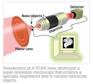
A*STAR researchers and collaborators at the National University of Singapore have developed a non-invasive optical microscope that can image smaller objects than conventional microscopes, and does not require samples to be dyed.
It is hard to overestimate the incredible contribution the humble optical microscope has made to science and industry. But microscopes suffer from a fundamental limitation that prevents them from distinguishing between two objects that are closer than about 200 nanometers. In recent years, various ingenious ways to overcome this limit have been demonstrated, but most of them require either placing the lens extremely close to the sample — both of which could be damaged during focusing — or staining the sample with fluorescent dyes, reducing the usefulness of these so-called super-resolution microscopes.
Now, Jinghua Teng of the A*STAR Institute of Materials Research and Engineering and colleagues have developed a super-resolution microscope that can distinguish objects separated by just 65 nanometers and does not suffer from either disadvantage.
The microscope has a specially engineered lens, known as a supercritical lens. This flat lens has transparent concentric rings at certain radii and focuses down to a much narrower spot than a conventional lens. By using this lens to focus a laser beam and then scanning the focused beam across a sample, it is possible to build up a high-resolution image of the sample. While other research groups have fabricated supercritical lenses in the past five years, they have various drawbacks. Teng and his team have overcome these disadvantages through improved lens design based on computer simulations.
Besides enabling super-resolution imaging, the lens has several other important advantages. It is easy and inexpensive to make because, unlike previous supercritical lenses, it has micrometer-scale features rather than nanometer-scale features. It also has a long, needle-like focal region, meaning that samples will remain in focus even if they move slightly up or down relative to the lenses. Furthermore, the distance between the lens and the sample is about ten times greater than that for previous supercritical lenses. Finally, since the imaging process is completely physical and captured in real time, there is no need for special sample preparation or mathematical post-processing of images, making the microscope quick and easy to use.
The team compared the performance of their microscope with those of a conventional optical microscope and a confocal laser scanning microscope, and found that theirs had superior resolution to both.
“This technique is highly attractive for developing the next generation of confocal laser scanning microscopes. There are huge potentials for planar-lens technology in general,” notes Teng. “We hope to commercialize the planar-lens technology within three to five years. We’re already having discussions with optic companies,” he adds. The researchers are working on optimizing the specifications of their microscope in preparation for commercialization.
Share on:


Testimonial
"Advertising in PCB007 Magazine has been a great way to showcase our bare board testers to the right audience. The I-Connect007 team makes the process smooth and professional. We’re proud to be featured in such a trusted publication."
Klaus Koziol - atgSuggested Items
Advint Incorporated Brings Artificial Intelligence to Electroplating Training
09/11/2025 | Advint IncorporatedAdvint Incorporated is introducing a new dimension to its electroplating training programs: the integration of Artificial Intelligence (AI). This initiative reflects the company’s commitment to providing PCB fabricators and manufacturers in the USA and Canada with training that is practical, forward-looking, and directly relevant to today’s production challenges.
The Signal Integrity Issue: Design007 Magazine September 2025
09/09/2025 | I-Connect007 Editorial TeamAs the saying goes, “If you don’t have signal integrity problems now, you will eventually.” This month, our experts share a variety of design techniques that can help PCB designers and design engineers achieve signal integrity.
Semiconductors Get Magnetic Boost with New Method from UCLA Researchers
07/31/2025 | UCLA NewsroomA new method for combining magnetic elements with semiconductors — which are vital materials for computers and other electronic devices — was unveiled by a research team led by the California NanoSystems Institute at UCLA.
SMT Perspectives and Prospects: Warren Buffett’s Perpetual Wisdom, Part 1
07/29/2025 | Dr. Jennie Hwang -- Column: SMT Perspectives and ProspectsOver the years, I have cherished the lessons by Warren Buffett and Charlie Munger at the Berkshire Hathaway annual shareholders meeting in Omaha, Nebraska. This year, I was among the more than 40,000 who attended the May 3 meeting. Millions more from around the world, including from the UK, Germany, Japan, China, Panama, and Guatemala, tuned in remotely and via CNBC’s livestream.
Mesa West, Advanced West Announce Strategic Partnership
06/15/2025 | I-Connect007Mesa West is proud to announce that they have officially joined forces with Advanced West. This strategic partnership brings together two industry leaders, uniting strengths to better serve customers through enhanced capabilities, expanded offerings, and continued commitment to quality.