


 American Made Advocacy: Five Years of Educating, Advocating, and Influencing Legislation and Policy
 Defense Speak Interpreted: Understanding What the Department of Defense Is, and Isn’t
 The Right Approach: The End of an Era—DoD Proposes MIL-PRF-31032 Cancellation


Miniaturization and increasing power densities are major concerns for modern electronic applications. The lifetime of electronic applications can be dramatically reduced by the increase of the working temperatures by just a few degrees. Further, the insulation of the whole printed circuit board (PCB) from the environment in order to provide efficient protection against humidity and dust for certain applications turns heat dissipation an even more challenging task.
State-of-the-art thermal management in the PCB is done by basically adding more copper to the PCB structure with constructions such as thick copper layers, Plated Through Holes (PTHs), copper filled laser vias or even copper inlays. Such methods can provide good heat dissipation, but can be also related to some disadvantages for several reasons: in the special case of thick copper planes for heat spreading, the production of the PCB becomes more costly and difficult since new equipment to handle the heavy thick copper panels is required. Besides, high-density packaging requires extreme fine copper lines in the PCB circuitry. This is not easily achieved when thick layers of copper are to be etched. In addition, weight is a major concern for aerospace applications and has become more attention for modern automotive concepts such as e-vehicles. Beyond that, large amounts of copper for cooling purposes can become very expensive. Thermal solutions such as modern miniaturized heat pipes which are light, have superior thermal conductive properties than copper and have sizes that are compatible with PCB dimensions can address thermal management challenges in modern high-end applications.
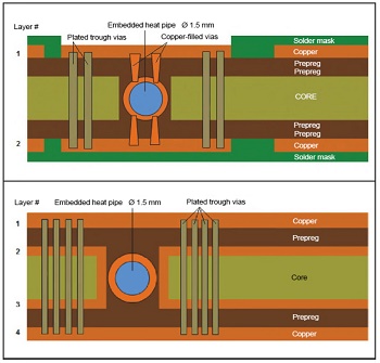
Heat pipes, due to their superior heat transfer capability with relatively small amount of mass, can guide heat very efficiently throughout the PCB plane. Modern heat pipes are small enough to be incorporated to PCB constructions. Their thickness can range from about 400 µm up to 2 mm. AT&S uses its know- how in embedding components and in 2.5D technology in order to associate mini heat pipes with the PCB. The application of heat pipes directly in the PCB body allows new design freedom such as remote cooling, heat guiding and heat spreading. For example, heat guiding may open room for the implementation of temperature sensitive components such as sensors and MEMS close to heat generating devices such as transistors. Further, the enhanced cooling capabilities of embedded heat pipes PCBs (HP-PCBs) may allow devices to run at lower temperatures which will in turn increase efficiency, lifetime and energy savings to most of electronic applications.
The embedded/inserted heat pipe is a passive component able to transport heat at large distances in the PCB more efficiently than any classical heat conductors (ex.: copper). Its heat transport mechanism is based on phase change (i.e. liquid-gas transformation) and mass transport. The heat pipe is a tubular structure sealed on both ends with an enclosed liquid at very low pressures. Normally, the tube is made of copper and water is the used liquid. When one end of the tube is heated, the water “changes phase” (in simple terms: becomes vapor), the increase of vapor pressure drives the vaporized water to the cold end of the tube. There, the water vapor releases energy and turns again into liquid. Capillary forces drag the liquid water back to the hot end of the tube. This dynamic process is repeated continuously and results in heat-transfer capabilities ranging from 100 to several thousand times that of a piece of copper with equivalent size. Since the heat pipe is a hollow structure, it has the additional advantage of being much lighter than copper rods.
AT&S demonstrated an innovative approach of associating “ready-to-use” mini heat pipes to the PCB body turning it into a complete heat management module. Various PCB demonstrator samples with embedded and inserted heat pipes were manufactured. Different strategies were used to associate miniature heat pipes with the PCB. In all experiments, the HP-PCB concept helped increasing the system’s overall thermal performance in comparison with current technologies. This technology is considered a thermal solution to virtually any electronic application where enhanced heat spreading or heat guiding is required. Potential in applications are specially found where weight and space are restrictive. Examples can be found in aviation, automotive and modern server applications.
AT&S R&D is actively looking for partners who have special challenges regarding thermal solutions for their future products and are willing to test the HP-PCB technology as early adopters. In its vision, modern PCBs must have enhanced functionalities (such as enhanced heat management, embedded components, high frequency materials, material hybridization etc.) which will become part of the solution to any technological challenge future applications might have.
About AT&S
AT&S is the European market leader and one of the globally leading manufacturers of high-value printed circuit boards and IC substrates. AT&S industrialises leading-edge technologies for its core business segments Mobile Devices, Automotive, Industrial, Medical and Advanced Packaging. AT&S has a global presence, with production facilities in Austria (Leoben and Fehring) and plants in India (Nanjangud), China (Shanghai, Chongqing) and Korea (Ansan, near Seoul). The company employed an average of 9,526 people in the financial year 2016/17. For more, click here.


