


 Trouble in Your Tank: Implementing Direct Metallization in Advanced Substrate Packaging
 It’s Only Common Sense: Storytelling That Sells—Stop Pitching, Start Painting Pictures
 The Right Approach: Get Ready for ISO 9001 Version 6


Controlling Traffic on the Electron Highway: Researching Graphene
August 31, 2017 | Department of Energy, Office of ScienceEstimated reading time: 9 minutes
On an otherwise normal day in the lab, Eva Andrei didn't expect to make a major discovery. Andrei, a physics professor at Rutgers University, was using graphite – the material in pencils – to calibrate a scanning tunneling microscope. As part of the process, she turned on a very powerful magnetic field. When she looked up to see the material's electronic spectrum, she was astonished. "We saw huge, beautiful peaks up there, just incredible. And they didn't make any sense," she recalled.
Remembering a lecture she'd recently attended, she realized the graphite had separated out into sheets just one atom thick. This material, known as graphene, has bizarre electronic properties. But even for graphene, the spectrum she saw was strange. In fact, no one had ever seen anything like it before. As Andrei described it, her colleague "went berserk in the corridor and just yelled ‘Graphene!'" Andrei had made a serendipitous discovery – a new electric phenomenon.
This was neither the first nor last time that electrons' movement in graphene would surprise and elate scientists. One of the most impressive things about graphene is how fast electrons move through it. They travel through it more than 100 times faster than they do through the silicon used to make computer chips. In theory, this suggests that manufacturers could use graphene to make superfast transistors for faster, thinner, more powerful touch-screens, electronics, and solar cells.
But what makes graphene so amazing also hinders its use: Electrons flow through its honeycomb structure too easily. Unlike silicon, graphene lacks a bandgap. Bandgaps are the amount of energy an electron must gain to free itself from an atom and move to other atoms to conduct a current. Like a toll on a highway, electrons need to "pay" with energy to proceed. Electronic devices use bandgaps as gates to control where and when electrons flow. Lacking bandgaps, graphene's structure acts like an electron superhighway with no stop signs.
"Graphene's electrons are so wild and can't be tamed; it's hard to create a gap," said Andrei.
That lack of a bandgap makes graphene currently very difficult to use in modern electronics. Researchers supported by the Department of Energy's (DOE's) Office of Science are investigating ways to overcome this challenge and others to direct graphene's electron traffic.
Electrons Behaving Like Particles of Light
Materials that are just a few atoms thick act fundamentally different than larger amounts of the same material.
"The biggest challenge is having a reliable understanding of the properties of the materials," said Lilia Woods, a physics professor at the University of South Florida.
Even for a material that flat, graphene has some odd characteristics. In most materials, electrons move at different speeds. But in graphene, they all move at the same speed. In fact, electrons in graphene act as if they have no mass – like particles of light. That's one reason why the electrons move so fast and are so difficult to control.
Directing the Electron Traffic
Studying graphene's behavior is one thing. Figuring out how to manipulate it is another. Scientists have been pursuing several different ways to control the electrons in graphene: developing nanoribbons, stretching it, pairing it with boron nitride (another atom-tall material), and applying electrical charges to empty spaces in it. Scientists pursue multiple approaches because they don't know which one will work the best. In the meantime, each approach provides its own unique insight into graphene's basic properties.
Graphene Nanoribbons
Producing graphene nanoribbons is one way to make a material that's already unimaginably thin, even skinnier. These ribbons maintain many of graphene's positive characteristics while potentially giving scientists better control over how the electrons behave, including creating bandgaps.
"You can view these little ribbons as electronic circuit elements," said Michael Crommie, a physicist at DOE's Lawrence Berkeley National Laboratory (Berkeley Lab).
The investigation of nanoribbons began before scientists even got into the lab. Based on calculations, physicists theorized more than a decade ago that nanoribbons could offer new ways to manipulate graphene's electronic properties. Experimentalists have confirmed this idea by developing nanoribbons with consistent, clean edges.
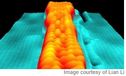
For example, researchers at the University of Wisconsin and elsewhere developed graphene nanoribbons that displayed a bandgap. They showed that when the width of a nanoribbon is smaller than three nanometers, about the thickness of a strand of DNA, it develops a significant bandgap. It also becomes a semiconductor. Unlike graphene's electron superhighway, semiconductors can switch back and forth between conducting electricity or not. The narrower the ribbon, the bigger the gap or the "energy toll" electrons need.
But one challenge is how to make a single nanoribbon that has multiple widths and therefore regions with different bandgaps. Nanoribbons of a single width won't give scientists the level of control needed to design complex circuitry. To solve this problem, Berkeley Lab scientists fused together segments of ribbon with different widths. This "bandgap engineering" is essential to manufacturing semiconductor devices and a big step towards using graphene in circuits.
These nanoribbons can't be used by themselves, so scientists are currently investigating how nanoribbons interact with different surfaces. University of South Florida researchers studied graphene nanoribbons on silicon carbide (SiC) substratesExternal link. They found that how certain edges of nanoribbons attach to the SiC substrate influence the bandgap. Nanoribbons with different widths and edges anchored on different substrates can allow scientists more control over electron properties than nanoribbons that aren't anchored at all.
Page 1 of 2
Share on:


Testimonial
"Advertising in PCB007 Magazine has been a great way to showcase our bare board testers to the right audience. The I-Connect007 team makes the process smooth and professional. We’re proud to be featured in such a trusted publication."
Klaus Koziol - atgSuggested Items
Advint Incorporated Brings Artificial Intelligence to Electroplating Training
09/11/2025 | Advint IncorporatedAdvint Incorporated is introducing a new dimension to its electroplating training programs: the integration of Artificial Intelligence (AI). This initiative reflects the company’s commitment to providing PCB fabricators and manufacturers in the USA and Canada with training that is practical, forward-looking, and directly relevant to today’s production challenges.
The Signal Integrity Issue: Design007 Magazine September 2025
09/09/2025 | I-Connect007 Editorial TeamAs the saying goes, “If you don’t have signal integrity problems now, you will eventually.” This month, our experts share a variety of design techniques that can help PCB designers and design engineers achieve signal integrity.
Semiconductors Get Magnetic Boost with New Method from UCLA Researchers
07/31/2025 | UCLA NewsroomA new method for combining magnetic elements with semiconductors — which are vital materials for computers and other electronic devices — was unveiled by a research team led by the California NanoSystems Institute at UCLA.
SMT Perspectives and Prospects: Warren Buffett’s Perpetual Wisdom, Part 1
07/29/2025 | Dr. Jennie Hwang -- Column: SMT Perspectives and ProspectsOver the years, I have cherished the lessons by Warren Buffett and Charlie Munger at the Berkshire Hathaway annual shareholders meeting in Omaha, Nebraska. This year, I was among the more than 40,000 who attended the May 3 meeting. Millions more from around the world, including from the UK, Germany, Japan, China, Panama, and Guatemala, tuned in remotely and via CNBC’s livestream.
Mesa West, Advanced West Announce Strategic Partnership
06/15/2025 | I-Connect007Mesa West is proud to announce that they have officially joined forces with Advanced West. This strategic partnership brings together two industry leaders, uniting strengths to better serve customers through enhanced capabilities, expanded offerings, and continued commitment to quality.