


 Trouble in Your Tank: Implementing Direct Metallization in Advanced Substrate Packaging
 It’s Only Common Sense: Storytelling That Sells—Stop Pitching, Start Painting Pictures
 The Right Approach: Get Ready for ISO 9001 Version 6


New Quantum Phenomena in Graphene Superlattices
September 19, 2017 | Graphene FlagshipEstimated reading time: 2 minutes
A team of Graphene Flagship researchers led by the University of Manchester reported in the journal Science showing the first new type of quantum oscillation to be reported for thirty years. This occurs by applying a magnetic field and it is the first of its kind to be present at high temperature and on the mesoscale. This research also sheds light on the Hofstadter butterfly phenomenon.
Quantum theory is the study of physics at the atomic and sub atomic level. It quantises energy and momentum and shows how objects are characterised as both particles and waves. Quantum oscillations can be used to map the properties of new materials in the presence of a magnetic field. This paper shows how it is possible to tune the magnetic field applied to a heterostructure comprising of graphene and boron nitride to create a whole host of different electronic materials.
The superlattice, created in graphene by its exact placement with regards to a periodically arranged boron nitride layer, interacts with the magnetic field in such a way that it is possible to tune its oscillation to manufacture bands and gaps in its electronics structure – meaning that the magnetic field can be used to tune the materials to be metallic, semiconducting or conducting.
Andre Geim, a leading member of the team and the 2010 Nobel Laureate, says “Oscillatory quantum effects always present milestones in our understanding of materials properties. They are exceedingly rare. It is more than 30 years since a new type of quantum oscillation was reported.” He added “Our oscillations stand out by their extreme robustness, happening under ambient conditions in easily accessible magnetic fields.”
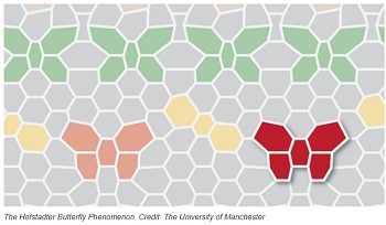
This work also sheds further light on Hofstadter’s butterfly, a fractal pattern that describes the behaviour of electrons in a magnetic field, measured experimentally for the first time in 2013 using a graphene and boron-nitride heterostructure. In the original theoretical work on which Hofstadter’s butterfly is based the electrons modelled to create the fractal pattern were treated as Bloch electrons (electrons that do not interact with one another and move within a periodic electric potential within a lattice). The research shown here illustrates how these complex fractal patterns can be viewed as Langmuir quantisation which is the quantisation of cyclotron orbits (taking what is normally thought of as a circular orbit and instead viewing it as linear).
Professor Vladimir Falko, Director of the National Graphene Institute commented “Our work helps to demystify the Hofstadter butterfly. The complex fractal structure of the Hofstadter butterfly spectrum can be understood as simple Landau quantisation in the sequence of new metals created by magnetic field.”
Professor Bart van Wees, Head of the Physics of Nanodevices group at the Zernike Institute for Advanced Materials, Groningen, The Netherlands added “We have always considered quantum oscillations as very brittle, easily destroyed at higher temperatures but the authors have shown that these can now be observed at room temperature, or even higher. This is good news for possible new applications of these and other systems which are based on Van der Waals stacking of two-dimensional materials.”
Share on:


Testimonial
"The I-Connect007 team is outstanding—kind, responsive, and a true marketing partner. Their design team created fresh, eye-catching ads, and their editorial support polished our content to let our brand shine. Thank you all! "
Sweeney Ng - CEE PCBSuggested Items
September 2025 PCB007 Magazine: The Future of Advanced Materials
09/16/2025 | I-Connect007 Editorial TeamMoore’s Law is no more, and the advanced material solutions being developed to grapple with this reality are surprising, stunning, and perhaps a bit daunting. Buckle up for a dive into advanced materials and a glimpse into the next chapters of electronics manufacturing.
I-Connect007 Launches Advanced Electronics Packaging Digest
09/15/2025 | I-Connect007I-Connect007 is pleased to announce the launch of Advanced Electronics Packaging Digest (AEPD), a new monthly digital newsletter dedicated to one of the most critical and rapidly evolving areas of electronics manufacturing: advanced packaging at the interconnect level.
Panasonic Industry will Double the Production Capacity of MEGTRON Multi-layer Circuit Board Materials Over the Next Five Years
09/15/2025 | Panasonic Industry Co., Ltd.Panasonic Industry Co., Ltd., a Panasonic Group company, announced plans for a major expansion of its global production capacity for MEGTRON multi-layer circuit board materials today. The company plans to double its production over the next five years to meet growing demand in the AI server and ICT infrastructure markets.
Trouble in Your Tank: Implementing Direct Metallization in Advanced Substrate Packaging
09/15/2025 | Michael Carano -- Column: Trouble in Your TankDirect metallization systems based on conductive graphite are gaining popularity throughout the world. The environmental and productivity gains achievable with this process are outstanding. Direct metallization reduces the costs of compliance, waste treatment, and legal issues related to chemical exposure. A graphite-based direct plate system has been devised to address these needs.
Fresh PCB Concepts: Designing for Success at the Rigid-flex Transition Area
08/28/2025 | Team NCAB -- Column: Fresh PCB ConceptsRigid-flex PCBs come in all shapes and sizes. Manufacturers typically use fire-retardant, grade 4 (FR-4) materials in the rigid section and flexible polyimide materials in the flex region. Because of the small size, some rigid-flex PCBs, like those for hearing aid devices, are among the most challenging to manufacture. However, regardless of its size, we should not neglect the transition area between the rigid and flexible material.