


 Flexible Thinking: Designing Flex Circuits for Dynamic Reliability
 Global PCB Connections: Rigid-flex and Flexible PCBs—The Backbone of Modern Electronics
 Happy’s Tech Talk #29: Bend-to-Install Semi-flex FR-4


Abstract
Printed electronics is a familiar term that is taking on more meaning as the technology matures. Flexible electronics is sometimes referred to as a subset of this and the printing approach is one of the enabling factors for roll-to-roll processes. Printed electronics is improving in performance and has many applications that compete directly with printed circuit boards. The advantage of roll-to-roll is the speed of manufacturing, the large areas possible, and a reduction in costs.
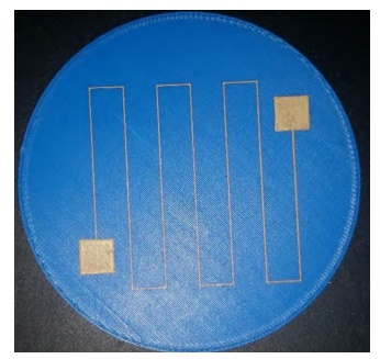
As this technology continues to mature, it is also merging with the high-profile 3D printing. 3D printing is becoming more than just a rapid prototyping tool and more than just printing small plastic toys. Companies are embracing 3D printing as a manufacturing approach to fabricate complex parts that cannot be done using traditional manufacturing techniques. The combination of 3D printing and printed electronics has the potential to make novel products and, more specifically, to make objects electrically functional. Electrically functional objects have the advantage of competing with printed circuit boards.
Printed circuit structures will be a new approach to electronic packaging. It is the desire of many companies to reduce assembly processes, decrease the size of the electronics, and do this at a reduced cost. This is challenging, but the potential of printing the structure and the electronics as a single monolithic unit has many advantages. This will reduce the human touch in assembly, as the electronics and the object are printed. This will increase the ruggedness of the product, as it is a monolithic device.
This will eliminate wires, solder, and connectors, making the device smaller. This has the potential to be the future of printed circuit boards and microelectronic packaging. This article will show working demonstrations of printed circuit structures, the obstacles, and the potential future of 3D printed electronics.
To read the full version of this article which appeared in the September 2017 issue of The PCB Magazine, click here.


