-
- News
- Books
Featured Books
- pcb007 Magazine
Latest Issues
Current IssueThe Hole Truth: Via Integrity in an HDI World
From the drilled hole to registration across multiple sequential lamination cycles, to the quality of your copper plating, via reliability in an HDI world is becoming an ever-greater challenge. This month we look at “The Hole Truth,” from creating the “perfect” via to how you can assure via quality and reliability, the first time, every time.
In Pursuit of Perfection: Defect Reduction
For bare PCB board fabrication, defect reduction is a critical aspect of a company's bottom line profitability. In this issue, we examine how imaging, etching, and plating processes can provide information and insight into reducing defects and increasing yields.
Voices of the Industry
We take the pulse of the PCB industry by sharing insights from leading fabricators and suppliers in this month's issue. We've gathered their thoughts on the new U.S. administration, spending, the war in Ukraine, and their most pressing needs. It’s an eye-opening and enlightening look behind the curtain.
- Articles
- Columns
- Links
- Media kit
||| MENU - pcb007 Magazine
Full Coverage of AltiumLive 2017
October 12, 2017 | I-Connect007Estimated reading time: Less than a minute

Altium recently conducted its first-ever users conference, AltiumLive 2017: Annual PCB Design Summit, at the Hilton Resort and Spa in San Diego. Speakers included Dan Beeker of NXP Semiconductors, Max Seeley of 3M Corporate R&D, Tara Dunn of OMNI PCB, Susy Webb of Fairfield Nodal, Charles Pfeil of Altium, and our own Happy Holden.
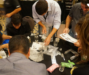
This conference drew hundreds of PCB designers, and included a robot design challenge and battle. If you couldn’t make it, don’t worry. We shot a variety of video and still photos.
To go directly to the interesting AltiumLive photo gallery, click here.
The next AltiumLive event takes place in Munich, Germany on October 24-25, 2017.
Watch the video of the robot challenge below or, click here.
Suggested Items
DownStream Acquisition Fits Siemens’ ‘Left-Shift’ Model
06/26/2025 | Andy Shaughnessy, I-Connect007I recently spoke to DownStream Technologies founder Joe Clark about the company’s acquisition by Siemens. We were later joined by A.J. Incorvaia, Siemens’ senior VP of electronic board systems. Joe discussed how he, Rick Almeida, and Ken Tepper launched the company in the months after 9/11 and how the acquisition came about. A.J. provides some background on the acquisition and explains why the companies’ tools are complementary.
Elementary Mr. Watson: Retro Routers vs. Modern Boards—The Silent Struggle on Your Screen
06/26/2025 | John Watson -- Column: Elementary, Mr. WatsonThere's a story about a young woman preparing a holiday ham. Before putting it in the pan, she cuts off the ends. When asked why, she shrugs and says, "That's how my mom always did it." She asks her mother, who gives the same answer. Eventually, the question reaches Grandma, who laughs and says, "Oh, I only cut the ends off because my pan was too small." This story is a powerful analogy for how many PCB designers approach routing today.
Siemens Turbocharges Semiconductor and PCB Design Portfolio with Generative and Agentic AI
06/24/2025 | SiemensAt the 2025 Design Automation Conference, Siemens Digital Industries Software today unveiled its AI-enhanced toolset for the EDA design flow.
Cadence AI Autorouter May Transform the Landscape
06/19/2025 | Andy Shaughnessy, Design007 MagazinePatrick Davis, product management director with Cadence Design Systems, discusses advancements in autorouting technology, including AI. He emphasizes a holistic approach that enhances placement and power distribution before routing. He points out that younger engineers seem more likely to embrace autorouting, while the veteran designers are still wary of giving up too much control. Will AI help autorouters finally gain industry-wide acceptance?
Beyond Design: The Metamorphosis of the PCB Router
06/18/2025 | Barry Olney -- Column: Beyond DesignThe traditional PCB design process is often time-consuming and labor-intensive. Routing a complex PCB layout can consume up to 30% of a designer’s time, and addressing this issue is not straightforward. We have all encountered this scenario: You spend hours setting the constraints and finally hit the Go button, only to be surprised by the lack of visual appeal and the obvious flaws in the result.