


 It’s Only Common Sense: The Importance of Setting Realistic Expectations
 Marcy’s Musings: The Relentless Pursuit of Perfection
 Dan’s Biz Bookshelf: ‘Do/Start'


Think Laterally to Sidestep Production Problems
October 16, 2017 | KAUSTEstimated reading time: 2 minutes
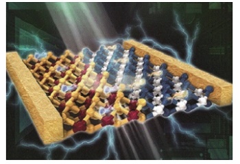
Super thin photovoltaic devices underpin solar technology and gains in the efficiency of their production are therefore keenly sought. KAUST researchers have combined and rearranged different semiconductors to create so-called lateral p-n heterojunctions—a simpler process they hope will transform the fabrication of solar cells, self-powered nanoelectronics as well as ultrathin, transparent, flexible devices.
Two-dimensional semiconductor monolayers, such as graphene and transition-metal dichalcogenides like WSe2 and MoS2, have unique electrical and optical properties that make them potential alternatives to conventional silicon-based materials. Recent advances in material growth and transfer techniques have allowed scientists to manipulate these monolayers. Specifically, vertical stacking has led to ultrathin photovoltaic devices but requires multiple complex transfer steps. These steps are hampered by various issues, such as the formation of contaminants and defects at the monolayer interface, which limit device quality.
“Devices obtained using these transfer techniques are usually unstable and vary from sample to sample,” says lead researcher and former visiting student of Associate Professor, Jr-Hau He, Meng-Lin Tsai, who adds that transfer-related contaminants significantly affect device reliability. Electronic properties have also proven difficult to control by vertical stacking.
To fully harness the exceptional properties of these two-dimensional materials, Tsai’s team, under the mentorship of He, created monolayers featuring lateral WSe2–MoS2 heterojunctions and incorporated them into solar cells. Under simulated sunlight, the cells achieved greater power conversion efficiency than their vertically stacked equivalents.
To do this, first the researchers synthesized the heterojunctions by consecutively depositing WSe2 and MoS2 on a sapphire substrate. Next, they transferred the materials onto a silicon-based surface for photovoltaic device fabrication.
High-resolution microscopy revealed that the lateral junction displayed a clear separation between the semiconductors at the interface. Also, the researchers detected no discernable height difference between semiconductor regions, consistent with an atomically thin interface.
These interfacial characteristics signaled success. “Our structures are cleaner and more ideal than vertically stacked assemblies because we didn’t need the multi-step transfer procedure,” explains Tsai.
Furthermore, the lateral heterojunctions mostly retained their efficiency despite changes to the orientation of the incident light. Being able to take light coming from any direction means expensive solar tracking systems will become redundant.
According to Tsai, the implementation of lateral heterojunctions in more complex circuits and interconnects may result in higher performance than in conventional solar cells and so the team is working on the next steps. “We are trying to understand the underlying kinetics and thermodynamics of these heterojunctions to design more efficient cells," he adds.
Share on:


Suggested Items
Electroninks Acquires Complete UTDots Advanced Materials Nanoinks Portfolio and IP
05/19/2025 | ElectroninksElectroninks, the leader in metal organic decomposition (MOD) inks for additive manufacturing and advanced semiconductor packaging, announced it has officially completed its full acquisition of UTDots products and IP into its portfolio, further expanding its offerings in digital printing for high-performance applications.
Future-proofing Electronics: ChemFORWARD Works Toward Collaboration for Safer Chemistry
05/19/2025 | Rachel Simon, ChemFORWARDThe electronics industry is facing a critical juncture. As consumer demand for sustainable products rises and regulatory pressures intensify, companies must prioritize the safety of their products and processes. This means not only complying with evolving chemical restrictions but also proactively seeking safer alternatives.
From DuPont to Qnity: A Bold Move in Electronics Materials
05/14/2025 | Marcy LaRont, I-Connect007DuPont has announced the intended spinoff of a public independent electronics company, Qnity, which will serve as a solutions provider to the semiconductor and electronics industries to enhance competitiveness and innovation in advanced computing, smart technologies, and connectivity. In this interview, Jon Kemp, Qnity CEO-elect and current president of DuPont’s Electronics business, shares his insights on the strategic separation from DuPont.
SMC Korea 2025 to Spotlight Next-Generation Memory and Materials Innovation amid AI Boom
05/13/2025 | SEMIThe Strategic Materials Conference (SMC) Korea 2025 is set to convene on May 14 at the Suwon Convention Center in Gyeonggi-do, South Korea, bringing together leading experts and innovators to highlight the critical role of materials innovation in addressing the performance, efficiency, and scalability requirements of AI-enabled semiconductor devices.
SEMI Applauds New Bill to Clarify Tax Credit Eligibility for Critical Semiconductor Suppliers Under U.S. CHIPS Act
05/12/2025 | SEMISEMI, the industry association serving the global semiconductor and electronics design and manufacturing supply chain, announced support of the Strengthening Essential Manufacturing and Industrial Investment Act (SEMI Investment Act), which clarifies that critical materials suppliers to semiconductor manufacturers are eligible for the Advanced Manufacturing Investment Tax Credit (“Section 48D”) created by the United States CHIPS and Science Act.