


 Global PCB Connections: Rigid-flex and Flexible PCBs—The Backbone of Modern Electronics
 Flexible Thinking: The Key to a Successful Flex Circuit Design Transfer
 Happy’s Tech Talk #29: Bend-to-Install Semi-flex FR-4


Think Laterally to Sidestep Production Problems
October 16, 2017 | KAUSTEstimated reading time: 2 minutes
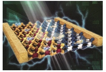
Super thin photovoltaic devices underpin solar technology and gains in the efficiency of their production are therefore keenly sought. KAUST researchers have combined and rearranged different semiconductors to create so-called lateral p-n heterojunctions—a simpler process they hope will transform the fabrication of solar cells, self-powered nanoelectronics as well as ultrathin, transparent, flexible devices.
Two-dimensional semiconductor monolayers, such as graphene and transition-metal dichalcogenides like WSe2 and MoS2, have unique electrical and optical properties that make them potential alternatives to conventional silicon-based materials. Recent advances in material growth and transfer techniques have allowed scientists to manipulate these monolayers. Specifically, vertical stacking has led to ultrathin photovoltaic devices but requires multiple complex transfer steps. These steps are hampered by various issues, such as the formation of contaminants and defects at the monolayer interface, which limit device quality.
“Devices obtained using these transfer techniques are usually unstable and vary from sample to sample,” says lead researcher and former visiting student of Associate Professor, Jr-Hau He, Meng-Lin Tsai, who adds that transfer-related contaminants significantly affect device reliability. Electronic properties have also proven difficult to control by vertical stacking.
To fully harness the exceptional properties of these two-dimensional materials, Tsai’s team, under the mentorship of He, created monolayers featuring lateral WSe2–MoS2 heterojunctions and incorporated them into solar cells. Under simulated sunlight, the cells achieved greater power conversion efficiency than their vertically stacked equivalents.
To do this, first the researchers synthesized the heterojunctions by consecutively depositing WSe2 and MoS2 on a sapphire substrate. Next, they transferred the materials onto a silicon-based surface for photovoltaic device fabrication.
High-resolution microscopy revealed that the lateral junction displayed a clear separation between the semiconductors at the interface. Also, the researchers detected no discernable height difference between semiconductor regions, consistent with an atomically thin interface.
These interfacial characteristics signaled success. “Our structures are cleaner and more ideal than vertically stacked assemblies because we didn’t need the multi-step transfer procedure,” explains Tsai.
Furthermore, the lateral heterojunctions mostly retained their efficiency despite changes to the orientation of the incident light. Being able to take light coming from any direction means expensive solar tracking systems will become redundant.
According to Tsai, the implementation of lateral heterojunctions in more complex circuits and interconnects may result in higher performance than in conventional solar cells and so the team is working on the next steps. “We are trying to understand the underlying kinetics and thermodynamics of these heterojunctions to design more efficient cells," he adds.
Share on:


Testimonial
"Advertising in PCB007 Magazine has been a great way to showcase our bare board testers to the right audience. The I-Connect007 team makes the process smooth and professional. We’re proud to be featured in such a trusted publication."
Klaus Koziol - atgSuggested Items
Fresh PCB Concepts: Designing for Success at the Rigid-flex Transition Area
08/28/2025 | Team NCAB -- Column: Fresh PCB ConceptsRigid-flex PCBs come in all shapes and sizes. Manufacturers typically use fire-retardant, grade 4 (FR-4) materials in the rigid section and flexible polyimide materials in the flex region. Because of the small size, some rigid-flex PCBs, like those for hearing aid devices, are among the most challenging to manufacture. However, regardless of its size, we should not neglect the transition area between the rigid and flexible material.
Global Sourcing Spotlight: How to Evaluate Supplier Capabilities Worldwide
08/20/2025 | Bob Duke -- Column: Global Sourcing SpotlightIn global sourcing, the difference between a competitive edge and a catastrophic disruption often comes down to how well you vet your suppliers. Sourcing advanced PCBs, precision components, or materials for complex assemblies demands diligence, skepticism, and more than a little time on airplanes. Here’s how to do your due diligence when evaluating international suppliers and why cutting corners can cost you more than money.
Insulectro and Electroninks Sign North American Distribution Agreement
08/12/2025 | InsulectroElectroninks, a leader in metal organic decomposition (MOD) inks for additive manufacturing and advanced semiconductor packaging, today announced a strategic collaboration and distribution partnership with Insulectro, a premier distributor of materials used in printed electronics and advanced interconnect manufacturing.
Happy’s Tech Talk #41: Sustainability and Circularity for Electronics Manufacturing
08/13/2025 | Happy Holden -- Column: Happy’s Tech TalkI attended INEMI’s June 12 online seminar, “Sustainable Electronics Tech Topic Series: PCBs and Sustainability.” Dr. Maarten Cauwe of imec spoke on “Life Cycle Inventory (LCI) Models for Assessing and Improving the Environmental Impact of PCB Assemblies,” and Jack Herring of Jiva Materials Ltd. spoke on “Transforming Electronics with Recyclable PCB Technology.” This column will review information and provide analysis from both presentations.
Dymax Renews Connecticut Headquarters Lease, Reinforces Long-Term Commitment to Local Community
08/08/2025 | DymaxDymax, a global manufacturer of rapid light-curing materials and equipment, is pleased to announce the renewal and extension of its corporate lease at its 318 Industrial Lane, Torrington, headquarters.